Optical coupling structure and substrate with built-in optical transmission function, and method of manufacturing the same

a technology of optical coupling structure and substrate, which is applied in the direction of optical elements, instruments, other domestic articles, etc., can solve the problems of not being able to increase the efficiency of optical coupling between surface-type optical semiconductor devices, a high signal vs. noise ratio (s/n ratio), and a high dynamic range of signal modulation. achieve high efficiency of optical coupling, efficiently enter the refraction index distributor, and efficiently transmit

Inactive Publication Date: 2009-12-10
KYOCERA CORP
View PDF10 Cites 4 Cited by
  • Summary
  • Abstract
  • Description
  • Claims
  • Application Information

AI Technical Summary

Benefits of technology

[0060]Further, in the optical coupling structure of the present invention, in the case when the optical path changing surface and the ends of the optical waveguides face each other at a distance, light transmitted from the optical path changing surface can be coupled with the optical waveguides so as to enter the ends thereof at right angles. Accordingly, it is possible to realize a highly efficient optical coupling between the refraction index distributors and the optical waveguides via the optical path changing surface.
[0061]Furthermore, in the optical coupling structure of the present invention, in the case when an optical semiconductor device is further included that optically couples with the optical waveguides via the refraction index distributors and the optical path changing surface, and has an active region facing the refraction index distributors, output light from the active region of the optical semiconductor device can be efficiently transmitted through the refraction index distributors by the light trapping effect of the refraction index distributors. Then, the output light efficiently enters the optical path changing surface, changes its light path to the direction of the optical axes of the optical waveguides by the optical path changing surface. Finally, the light can efficiently enter the refraction index distributors. Further, input light transmitted from the optical waveguides to the active region of the optical semiconductor device changes its optical path to the direction of the optical axes of the refraction index distributors by the optical path changing surface optically coupled with the optical waveguides. Then, the input light enters the refraction index distributors, is efficiently transmitted through the refraction index distributors by the light trapping effect of the refraction index distributors. Finally, the input light can efficiently enter the active region of the optical sem

Problems solved by technology

Along with these trends, the attenuation of signals in electric wires formed on a package board and cross talks among adjacent wires are increasing conspicuously, which is becoming a serious problem.
However, according to the optical coupling structure shown in FIG. 8, there is a problem that it is not possible to increase the efficiency of the optical coupling between the surface type optical semiconductor devices, or the laser diode 101 and the photo diode 102, and the optical waveguide which is the optical wire layer 103.
Accordingly, this has created a problem in the prior art that a high signal vs. noise ratio (S/N ratio) and a high dynamic range of signal modulation cannot be used.
In such case, low energy efficiency in the signal transmission cannot be avoided, which has been another problem in the prior art.
Accordingly, this may result in the necessity to add a complicated heat dissipat

Method used


Image

  • Optical coupling structure and substrate with built-in optical transmission function, and method of manufacturing the same
  • Optical coupling structure and substrate with built-in optical transmission function, and method of manufacturing the same
  • Optical coupling structure and substrate with built-in optical transmission function, and method of manufacturing the same

Examples


Embodiment Construction

[0076]The optical coupling structure and the substrate with a built-in optical transmission function and the method of manufacturing the same according to the present invention will now be described in more detail with reference to the accompanying drawings.

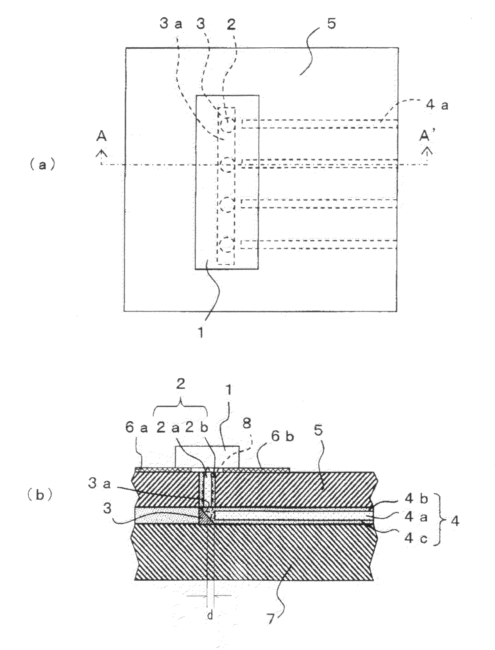
[0077]FIG. 1 is a diagram showing a schematic configuration in a preferred embodiment of the optical coupling structure and the substrate with a built-in optical transmission function equipped with the same according to the present invention. FIG. 1A is a top view of the substrate, and FIG. 1B is a cross sectional view taken along lines A-A′ in FIG. 1A.

[0078]In FIG. 1, reference numeral 1 denotes an optical semiconductor device, 2 denotes a refraction index distributor, 3 denotes an optical path changing portion having the optical path changing surface denoted by 3a, 4 denotes an optical waveguide, 4a denotes a core portion, 4b denotes an upper clad portion, and 4c denotes a lower clad portion. Further, 5 denotes an upper substra...


PUM


Abstract

To provide an optical coupling structure that can transmit signal light efficiently and change the light paths, and thereby increase the coupling efficiency of the optical coupling between an optical semiconductor device and optical waveguides.
An optical coupling structure is disclosed that includes optical waveguides optically coupled with an optical path converting surface that is arranged in substrates and an optical semiconductor device mounted on the upper substrate with its active region facing the optical path converting surface, which are optically coupled, via cylindrical refraction index distributors formed of a photosensitive polymer material, arranged so as to go through the portion between the active region of the optical semiconductor device and the optical path converting surface. It is possible to increase the coupling efficiency of the optical coupling between the optical semiconductor device and the optical waveguides, and to realize a high quality and high speed signal transmission at a high energy efficiency.

Description

[0001]This application is a U.S. national phase of International Application No. PCT / JP2006 / 308576 filed 24 Apr. 2006, which designated the U.S. and claims priority to JP 2005-126861 filed 25 Apr. 2005 and JP 2006-093062 filed 30 Mar. 2006, the entire contents of each of which are hereby incorporated herein by reference.BACKGROUND OF THE INVENTION[0002]1. Field of the Invention[0003]The present invention relates to an optical coupling structure including optical waveguides and optical transmitters arranged vertically thereto, a substrate with a built-in optical transmission function equipped with this optical coupling structure and a method of manufacturing the same.[0004]2. Description of the Related Art[0005]In order to increase the throughput in information processing and improve the processing speed, there is a trend to increase the operation speed of semiconductor devices and the number of signal input / output terminals for the future. At the same time, the number of signal wire...

Claims


Application Information

Patent Timeline
IPC IPC(8): G02B6/12G02B6/00G02B6/42B29D11/00
CPCG02B6/43G02B6/4214H01L2224/16225
Inventor MATSUBARA, TAKAHIRO
Owner KYOCERA CORP
Why Eureka
Try Eureka