Formation of solar cell-selective emitter using implant and anneal method

a technology of solar cells and emitters, applied in the field of solar cells, can solve the problems of lack of utilization of blue light, varying light absorption and electron-hole generation performance, and affecting the production of final products, so as to achieve the effect of improving performan

Inactive Publication Date: 2009-12-17
INTEVAC
View PDF100 Cites 90 Cited by
  • Summary
  • Abstract
  • Description
  • Claims
  • Application Information

AI Technical Summary

Benefits of technology

[0008]The present invention provides methods for addressing the various ohmic losses arising from the use of older processes of doping solar substrate. The present invention involves modifying the resistance of the substrate, contacts, busbars and fingers, the contact resistance of the metal-silicon interface, the resistance of backside metallization, and achieving the desired resistivity under the grid contact and in between the fingers. Moreover, the advantageous formation of a selective emitter and its ability to improve performance is possible through the use of the present invention. The present invention is capable of being applied to grown single or mono-crystalline silicon, poly or multi-crystalline silicon, as well as very thin silicon or very thin film deposited silicon or other materials used for solar cell formation and other applications. It is also capable of being extended to atomic species placement for any other material used in the fabrication of junctions and / or contacts.
[0009]Application-specific ion implantation and annealing systems and methods can be employed by the present invention in order to provide the appropriate and independent placement and concentration of dopant both within the bulk of the material and laterally positioned across the substrate. The use of accurate and highly accurately placed dopant and tailoring of dopant atomic profile is described below. Methods are described that address the requirements for heavily doped (10-40 Ohms / square) regions under the grid line, as well as methods to achieve lightly doped (80-160 Ohms / square) regions in between grid fingers. Ideal sheet resistance levels of approximately 25 Ohms / square for the contact region under the grid line, which translates to a dopant concentration of approximately 1E20 per cubic centimeter, and approximately 100 Ohms / square for the electron-hole pair generation region between the grid fingers and / or below the contact region, which translates to a dopant concentration of approximately 1E19 per cubic centimeter, are able to be achieved through the use of the present invention.
[0010]Additionally, through the use of tailored parameters, the atomic dopant profile is simultaneously matched to provide the electrical junctions at the appropriate depth against the substrate background doping levels and to provide the resistivity required for the formation of the contacts on the surface. Use of retrograde doping and flat atomic profile (box junctions) are also deployed, if desired. This methodology provides a simple, effective and inexpensive means for formation of a selective emitter and appropriate resistivity to enhance solar cells efficiency performance.
[0011]The dopants can be activated through the use of a traditional furnace anneal with long time anneal, the use of rapid annealing, such as rapid thermal anneal (RTA), or the use of very rapid temperature rise and cool down methods, such as laser annealing, flash lamp annealing, or employing a firing furnace at the end of the solar cell fabrication, which can employ a lower temperature when used with the implantation of the present invention. Controlled use of annealing time and temperature provides further enhancement of atomic profile within the substrate. In the present invention, shorter time anneal is preferably used to ensure that dopant placement is not altered, but that full or near full activation is achieved.

Problems solved by technology

The use of diffusion of dopant from the surface into the substrate is plagued by problems.
One of the main problems is the accumulation of unactivated dopants near the surface as the dopants are driven into the bulk of the material, which can vary the resistivity at different depths and regions of the substrate and thus lead to varying light absorption and electron-hole generation performance.
In particular, one problem encountered is the lack of utilization of the blue light as the result of formation of the so-called “dead layer.”
Additionally, lateral positioning of the dopants across the substrate is especially difficult as the line widths and wafer thicknesses are getting smaller.
Such placement can be very difficult for the present methodology of diffusion and screen printing.
Moreover, as wafers get thinner, from 150-200 microns of today down to less than 20 microns, vertical and batch diffusion and screen printing becomes extremely difficult or even impossible.
Furthermore, the use of diffusion has been unable to provide the ideal levels of dopant concentration and resulting resistivity.
Diffusion is unable to address each region separately and is limited to a sheet resistance of about 50 Ohms / square (Ω / □) for both regions, which is not quite high enough for the electron-hole pair generation region and not quite low enough for the contact region.

Method used


Image

  • Formation of solar cell-selective emitter using implant and anneal method
  • Formation of solar cell-selective emitter using implant and anneal method
  • Formation of solar cell-selective emitter using implant and anneal method

Examples


Embodiment Construction

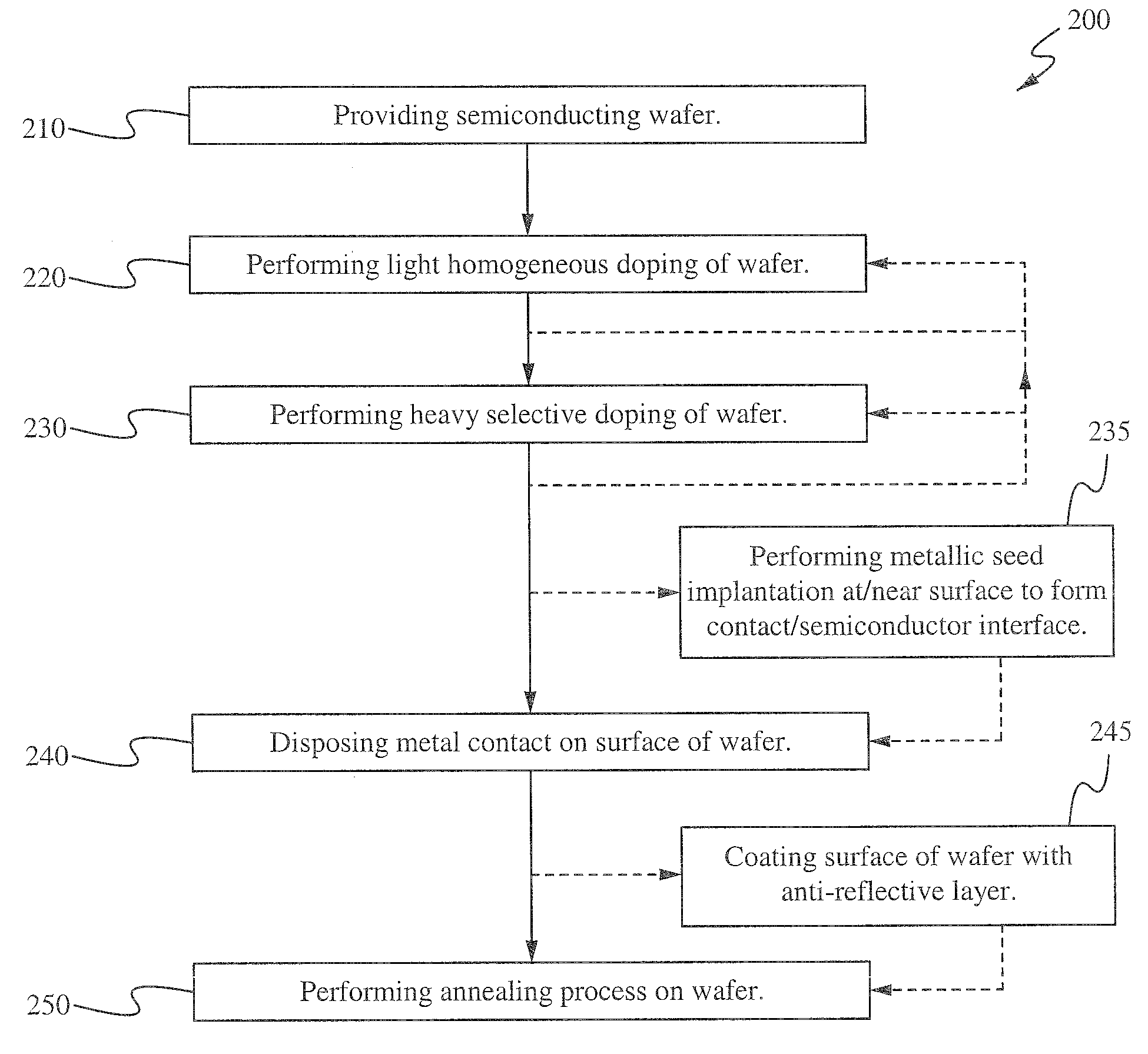
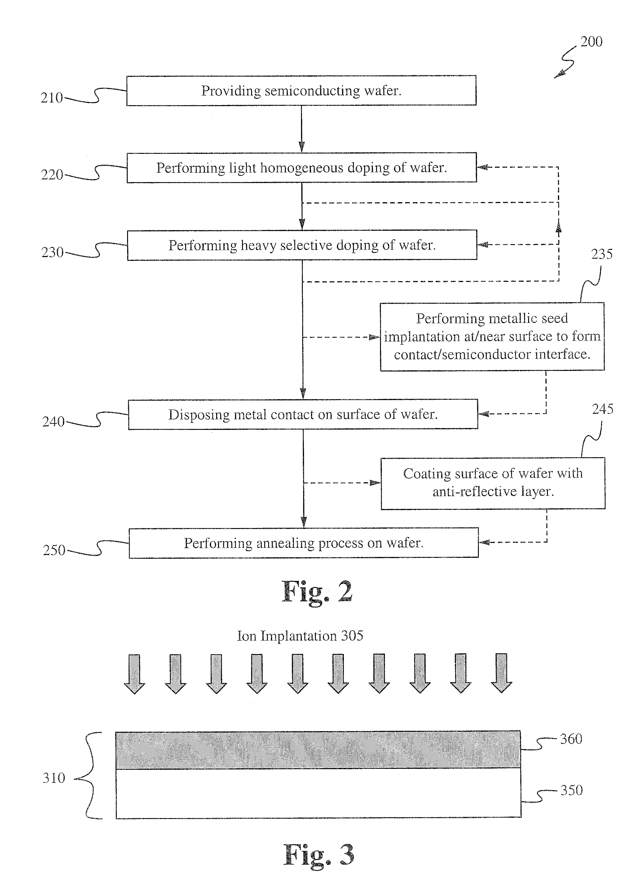
[0037]The following description is presented to enable one of ordinary skill in the art to make and use the invention and is provided in the context of a patent application and its requirements. Various modifications to the described embodiments will be readily apparent to those skilled in the art and the generic principles herein may be applied to other embodiments. Thus, the present invention is not intended to be limited to the embodiment shown but is to be accorded the widest scope consistent with the principles and features described herein.

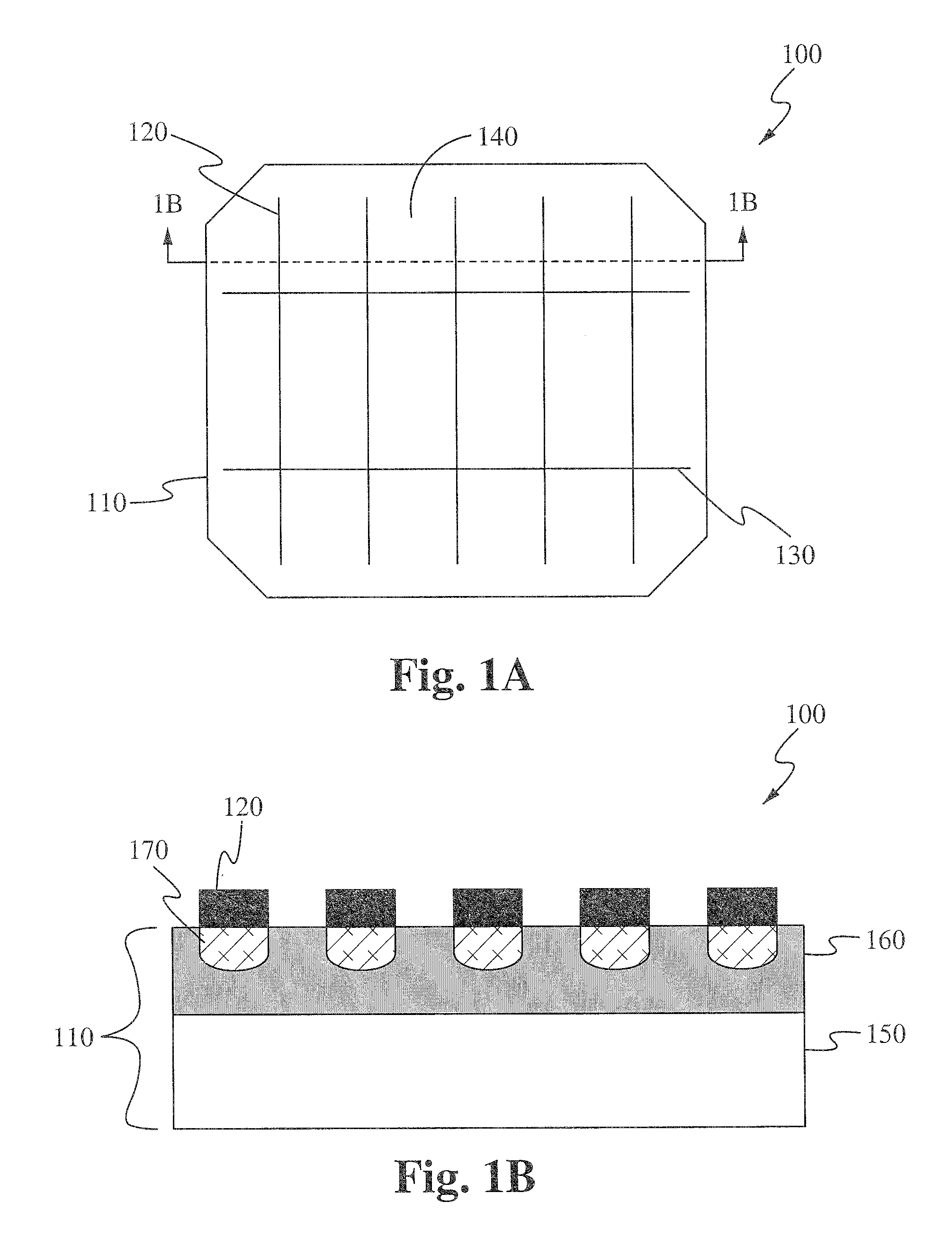
[0038]FIGS. 1A-10B illustrate embodiments of a solar cell device, its characteristics, and its formation, with like elements being numbered alike.

[0039]FIGS. 1A and 1B illustrate a plan view and a cross-sectional side view, respectively, of one embodiment of a solar cell 100 drawn to different scales in accordance with the principles of the present invention. The solar cell 100 comprises a wafer 110. In some embodiments, the wafer 110 is a 1...


PUM


Abstract

A method of forming a solar cell, the method comprising: providing a semiconducting wafer having a pre-doped region; performing a first ion implantation of a dopant into the semiconducting wafer to form a first doped region over the pre-doped region, wherein the first ion implantation has a concentration-versus-depth profile; and performing a second ion implantation of a dopant into the semiconducting wafer to form a second doped region over the pre-doped region, wherein the second ion implantation has a concentration-versus-depth profile different from that of the first ion implantation, wherein at least one of the first doped region and the second doped region is configured to generate electron-hole pairs upon receiving light, and wherein the first and second ion implantations are performed independently of one another.

Description

CROSS-REFERENCE TO RELATED APPLICATIONS[0001]This application claims priority to co-pending U.S. Provisional Application Ser. No. 61 / 131,687, filed Jun. 11, 2008, entitled “SOLAR CELL FABRICATION USING IMPLANTATION,” co-pending U.S. Provisional Application Ser. No. 61 / 131,688, filed Jun. 11, 2008, entitled “APPLICATIONS SPECIFIC IMPLANT SYSTEM FOR USE IN SOLAR CELL FABRICATIONS,” co-pending U.S. Provisional Application Ser. No. 61 / 131,698, filed Jun. 11, 2008, entitled “FORMATION OF SOLAR CELL-SELECTIVE EMITTER USING IMPLANTATION AND ANNEAL METHODS,” co-pending U.S. Provisional Application Ser. No. 61 / 133,028, filed Jun. 24, 2008, entitled “SOLAR CELL FABRICATION WITH FACETING AND IMPLANTATION,” and co-pending U.S. Provisional Application Ser. No. 61 / 210,545, filed Mar. 20, 2009, entitled “ADVANCED HIGH EFFICIENCY CRYSTALLINE SOLAR CELL FABRICATIONS METHOD,” which are all hereby incorporated by reference as if set forth herein.FIELD OF THE INVENTION[0002]The present invention relate...

Claims


Application Information

Patent Timeline
Patent Type & Authority Applications(United States)
IPC IPC(8): H01L31/00H01L31/0352H01L21/24H01L21/22
CPCH01L21/26513H01L21/266Y02E10/547H01L31/072H01L31/1804H01L31/022425H01L21/2658Y02P70/50H01L31/04H01L31/18H01L21/265H01L31/0236H01L21/26506
Inventor ADIBI, BABAKMURRER, EDWARD S.
Owner INTEVAC
Why Eureka
Try Eureka