Display
a technology of display and screen, applied in the field of display, can solve the problems of reduced luminance, low stability, and organic electroluminescence devices, and achieve the effects of improving sealing characteristics, good sidewall step coverage, and low density
- Summary
- Abstract
- Description
- Claims
- Application Information
AI Technical Summary
Benefits of technology
Problems solved by technology
Method used
Image
Examples
example 1
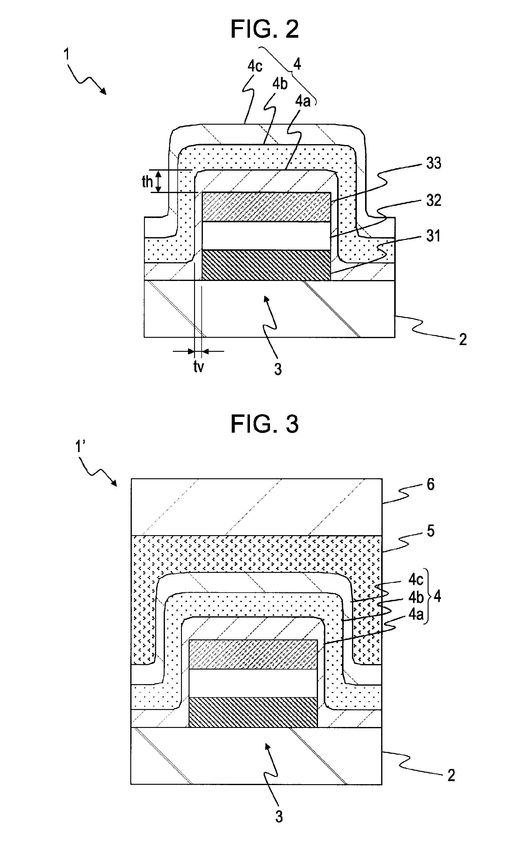
[0067]In Example 1, a display 1 having the configuration shown in FIG. 2 was formed. In this example, the protective film 4 was provided by laminating the high-density silicon nitride film 4a formed under the condition 2 of the comparative example, the low-density silicon nitride film 4b formed under the condition 3, and the high-density silicon nitride film 4c formed under the condition 2 in that order. In order to form the protective film 4, the silicon nitride films 4a, 4b, and 4c were continuously deposited by the plasma CVD method.
[0068]FIG. 12 shows the results of measurement of the life time of the organic electroluminescence devices 3 in the display 1 formed in Example 1. FIG. 12 also shows the lifetimes measured for the samples 1 and 4 of the comparative example.
[0069]As shown in FIG. 12, it was confirmed that the display 1 of Example 1 has good lifetime equivalent to that of the sample 1 using the high-density silicon nitride film and maintains good sealing characteristics...
example 2
[0074]In Example 2, a display 1′ with the configuration shown in FIG. 3 was formed. In this example, the epoxy resin 5 was applied over the entire surface of the protective film 4 of the display formed in Example 1, and a glass substrate (sealing substrate) 6 was bonded with the epoxy resin 5 used as an adhesive.
[0075]As a result of a test in which the display 1′ of Example 2 formed described above was exposed in a high-temperature and high-humidity atmosphere of a temperature of 80° C. and a humidity of 75%, moisture penetration between the substrate 2 and the glass substrate 6 was not observed. As a result of the same test of the display 1 of Example 1, a mark of moisture penetration was observed in a portion of silicon nitride (within the protective film 4) 2 mm or more inside the edge of the substrate 2. Therefore, it was confirmed that moisture penetration in the display can be suppressed by bonding the sealing substrate 6 through the resin 5.
example 3
[0076]In Example 3, a display 1 having the configuration shown in FIG. 2 was formed. In this example, the protective film 4 was provided by laminating the high-density silicon nitride film 4a formed under the condition 2 of the comparative example, the low-density silicon nitride film 4b formed under the condition 3, and the high-density silicon nitride film 4c formed under the condition 1 in that order. Namely, the films were deposited under the condition 2 / condition 3 / condition 1 in the order from the lower layer side. In order to form the protective film 4, the silicon nitride films 4a, 4b, and 4c were continuously deposited by the plasma CVD method.
[0077]As a result of a test in which the display 1 of Example 3 formed described above was exposed in a high-temperature and high-humidity atmosphere of a temperature of 80° C. and a humidity of 75%, a mark of moisture was not observed in a portion of silicon nitride (within the protective film 4) 2 mm or more inside the edge of the s...
PUM
 Abstract
Description
Claims
Application Information


