

Variable Capacitance Capacitor Array, Variable Capacitance Capacitor Array Device and Circuit Module
a capacitor array and variable capacitance technology, applied in the direction of mechanically variable capacitors, variable capacitors, one-port networks, etc., can solve the problems of limiting the control of the tunability through the thickness of the film, failure to meet a still higher tunability requirement, and deterioration of the film thickness, so as to increase the applicable frequency range or power range, broaden the applicable temperature range, and broaden the effect of utility
- Summary
- Abstract
- Description
- Claims
- Application Information
AI Technical Summary
Benefits of technology
Problems solved by technology
Method used
Image

Examples
first example
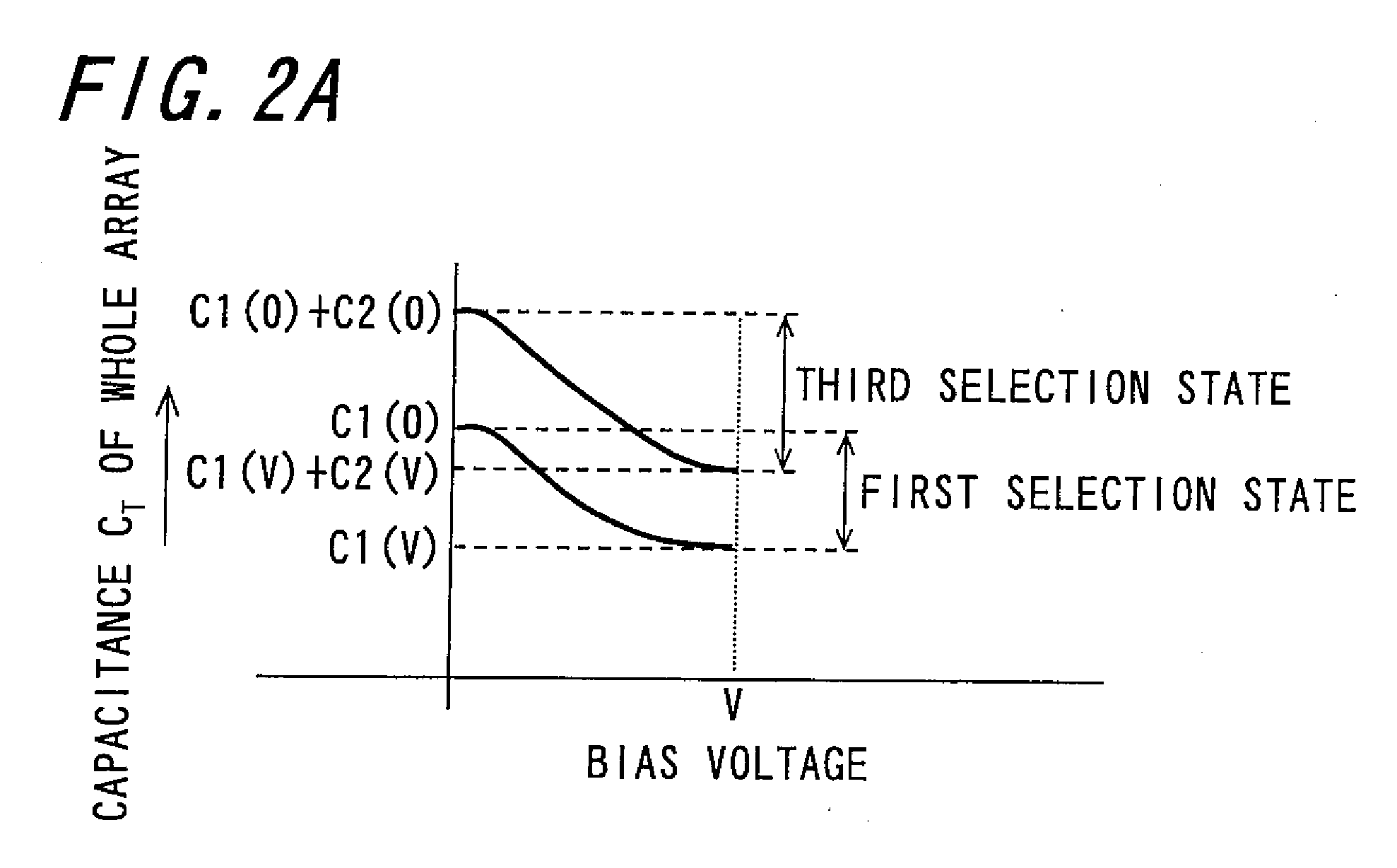
[0037]FIG. 2A shows the relationship between the capacitance CT of the whole variable capacitor array and the bias voltage in the variable capacitor array of the invention where the capacitance values of the first variable capacitor C1 and the second variable capacitor C2 satisfy the following expressions (1) and (2).
C1(0)≧C2(0) (1)
C1(0)≧C1(V)+C2(V) (2)
[0038]wherein, as described above, C1(0) and C1(V) respectively represent the capacitances of the first variable capacitor before and after voltage application, and C2(0) and C2(V) respectively represent the capacitances of the second variable capacitor before and after voltage application.
[0039]As shown in FIG. 2A, when one of the first and the third selection states is selected by switching between the first selection state and the third selection state under the condition that the expressions (1) and (2) are satisfied, the variable capacitance range in the third selection state and the variable capacitance range in the first sele...
second example
[0056]FIG. 2B shows the relationship between the capacitance CT of the whole variable capacitor array and the bias voltage in the variable capacitor array of the invention where the capacitance values of the first variable capacitor C1 and the second variable capacitor C2 satisfy all the following expressions (3) and (4).
C1(0)≧C2(0) (3)
C2(0)≧C1(V) (4)
[0057]wherein C1(0) and C1(V) respectively represent the capacitances of the first variable capacitor before and after voltage application, and C2(0) and C2(V) respectively represent the capacitances of the second variable capacitor before and after voltage application.
[0058]As shown in FIG. 2B, when one selection state is selected by switching between the first selection state and the second selection state under the condition that the expressions (3) and (4) are satisfied, the variable capacitance range in the first selection state and the variable capacitance range in the second selection state partially overlap with each other, wh...
third example
[0068]FIG. 2C shows the relationship between the capacitance CT of the whole variable capacitor array and the bias voltage in the variable capacitor array of the invention where the capacitance values of the first variable capacitor C1 and the second variable capacitor C2 satisfy all the following expressions (5) to (7).
C1(0)≧C2(0) (5)
C1(0)≧C1(V)+C2(V) (6)
C2(0)≧C1(V) (7)
[0069]wherein C1(0) and C1(V) respectively represent the capacitances of the first variable capacitor before and after voltage application, and C2(0) and C2(V) respectively represent the capacitances of the second variable capacitor before and after voltage application.
[0070]As shown in FIG. 2C, under the condition that the expressions (5) to (7) are satisfied, the variable capacitance range in the third selection state and the variable capacitance range in the first selection state partially overlap with each other, and the variable capacitance range in the first selection state and the variable capacitance range...
PUM
 Abstract
Description
Claims
Application Information