Post oxidation annealing of low temperature thermal or plasma based oxidation

Inactive Publication Date: 2009-12-17
APPLIED MATERIALS INC
View PDF19 Cites 20 Cited by
  • Summary
  • Abstract
  • Description
  • Claims
  • Application Information

AI Technical Summary

Benefits of technology

[0012]Embodiments of the present invention provide methods of forming oxide layers on semiconductor substrates. In some embodiments, a method of forming an oxide layer on a semiconductor substrate includes forming an oxide layer on a substrate using an oxidation process having a first process gas at a first temperature less than about 800 degrees Celsius; and annealing the oxide layer formed on the substrate in the presence of a second process gas and at a second

Problems solved by technology

Unfortunately, as feature sizes are becoming much smaller and different oxides are employed in the next generation of advanced technologies, the high wafer temperatures required in thermal oxidation processes are problematic in that the sharp junction definitions which are now required become diffused at the higher temperatures (e.g., above about 800 degrees Celsius).
Such a distortion of junction definitions and other features can lead to poor device performance or failure.
Thermal oxidation processes at higher temperatures (e.g., above about 800 degrees Celsius), for example, can cause unwanted metal oxidation in exposed metal layers (e.g., tungsten, tantalum).
Additionally, for example, during sidewall polysilicon re-oxidation of a polysilicon gate structure, higher temperature oxidation can cause polysilicon grain coarsening that can lead to poor device performance.
Plasma oxidation processes used to form oxide layers have similar problem

Method used


Image

  • Post oxidation annealing of low temperature thermal or plasma based oxidation
  • Post oxidation annealing of low temperature thermal or plasma based oxidation
  • Post oxidation annealing of low temperature thermal or plasma based oxidation

Examples


Embodiment Construction

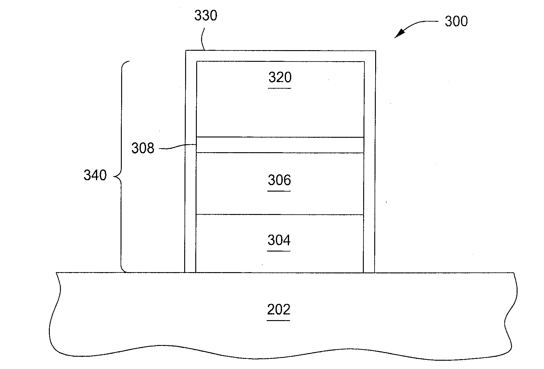
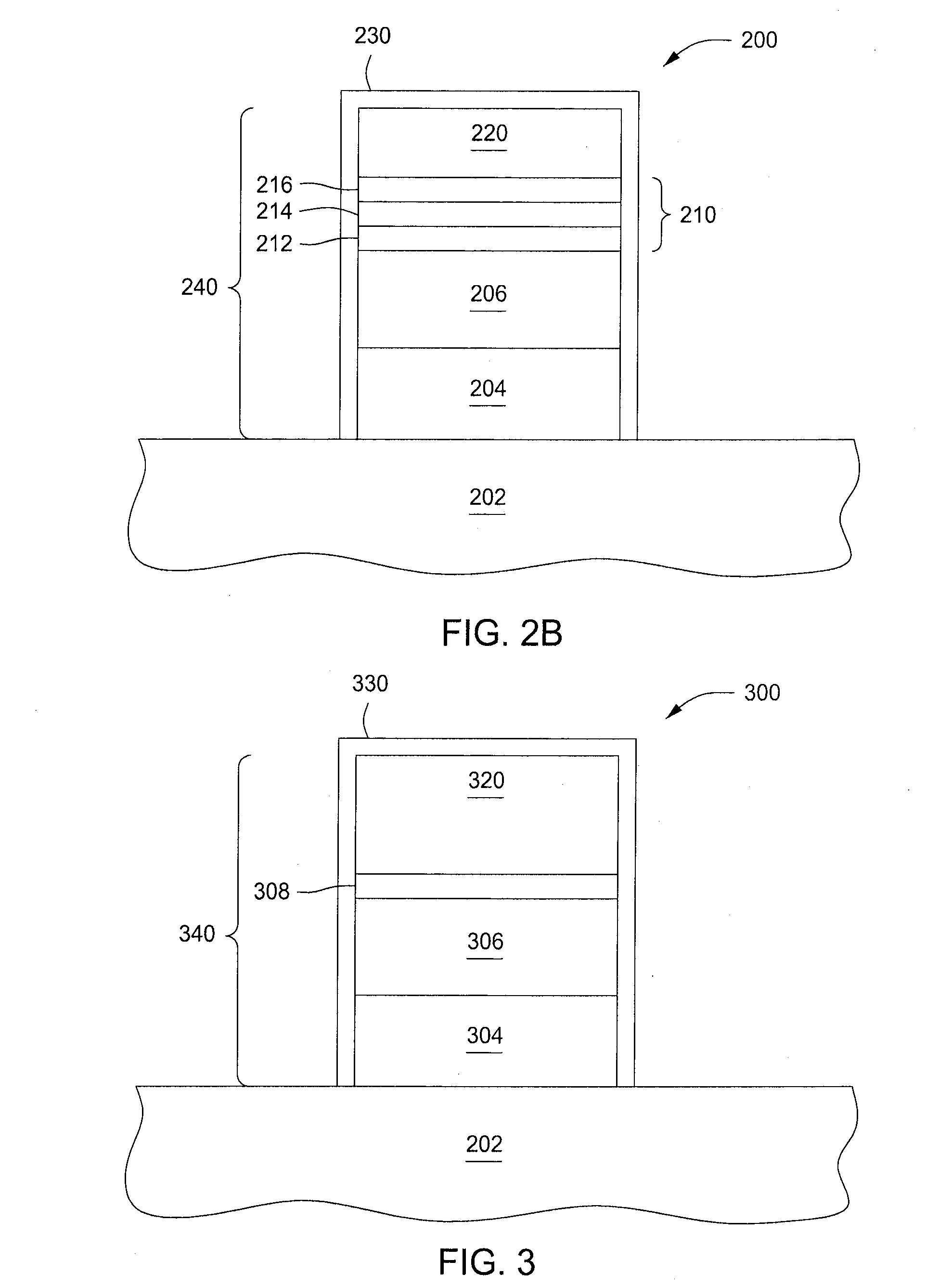
[0019]Embodiments of the present invention provide methods for the fabrication of oxide layers on semiconductor substrates. The inventive processes may advantageously provide formation of oxide layers with low impurities, reduced dopant diffusion, reduced poly silicon grain coarsening, and reduced metal oxidation as compared to conventional processes. In some embodiments of the present invention, oxide layers, such as a gate stack oxidation layer may be formed (e.g., an oxide layer deposited atop and along the exposed surfaces of a gate stack) upon a gate stack as utilized in logic and memory (such as dynamic random access memory, or DRAM, and FLASH) applications. As used herein, the phrase “forming an oxide layer on a substrate” includes total, partial, and selective oxidation processes performed on flat substrates and on structures formed on substrates, such as, for example, the tops and / or sidewalls of gate stacks disposed on the substrate.

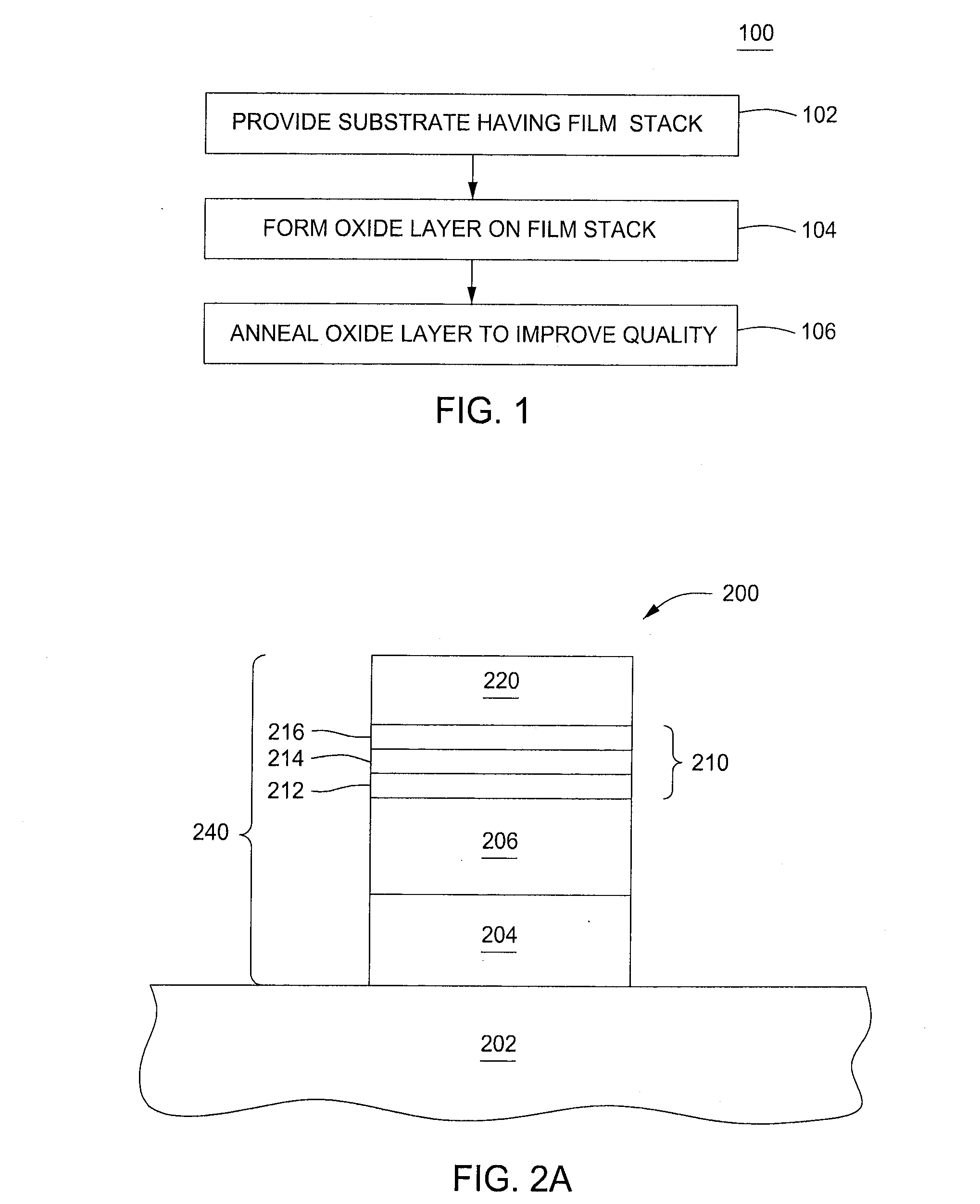
[0020]FIG. 1 depicts a method 100 for fo...


PUM


Abstract

Embodiments of the present invention provide methods of forming oxide layers on semiconductor substrates. In some embodiments, a method of forming an oxide layer on a semiconductor substrate includes forming an oxide layer on a substrate using an oxidation process having a first process gas at a first temperature less than about 800 degrees Celsius; and annealing the oxide layer formed on the substrate in the presence of a second process gas and at a second temperature. The oxidation process may be a plasma or thermal oxidation process performed at a temperature of about 800 degrees Celsius or below. In some embodiments, the post oxidation annealing process may be a spike or soak rapid thermal process, a laser anneal, or a flash anneal performed at a temperature of at least about 700 degrees Celsius, at least about 800 degrees Celsius, or at least about 950 degrees Celsius.

Description

CROSS-REFERENCE TO RELATED APPLICATIONS[0001]This application claims benefit of U.S. provisional patent application Ser. No. 61 / 061,603, filed Jun. 14, 2008, which is herein incorporated by reference.BACKGROUND OF THE INVENTION[0002]1. Field of the Invention[0003]Embodiments of the present invention generally relate to semiconductor fabrication, and more particularly, to oxidation of a semiconductor device or its components.[0004]2. Description of the Related Art[0005]Semiconductor devices require thin oxide layers to be formed at various stages of their fabrication. For example, in transistors, a thin gate oxide layer may be formed as part of a gate stack structure. In addition, in some applications, such as in the fabrication of a flash memory film stack, a thin oxide layer may be formed surrounding the entire gate stack, for example, via exposing the stack to an oxidation process. Such oxidation processes have conventionally been performed either thermally or using a plasma.[0006...

Claims


Application Information

Patent Timeline
IPC IPC(8): H01L21/316
CPCH01L21/0223H01L21/02238H01L21/02252H01L21/02255H01L29/517H01L21/28247H01L21/28273H01L21/28282H01L21/31662H01L21/02337H01L29/40114H01L29/40117
Inventor OLSEN, CHRISTOPHER S.YOKOTA, YOSHITAKAMANI, RAJESHSWENBERG, JOHANES
Owner APPLIED MATERIALS INC
Why Eureka
Try Eureka