Power Transfer Device, Power Supply Device and Power Receiving Device

a power transfer device and power supply technology, applied in the direction of fixed transformers or mutual inductances, circuit arrangements, inductances, etc., can solve the problems of difficult to make the coupling constant equal to 1, the transformer has a coupling constant of 1 not suitable for non-contact power transfer, and the energy transfer efficiency of the transformer also decreases. , to achieve the effect of improving the transfer efficiency

Active Publication Date: 2009-12-31
SONY CORP
View PDF9 Cites 29 Cited by
  • Summary
  • Abstract
  • Description
  • Claims
  • Application Information

AI Technical Summary

Benefits of technology

[0006]However, a transformer having a coupling constant of 1 is not suitable for non-contact power transfer because it is coupled by its magnetic material core forming a closed magnetic circuit. On the other hand, with a transformer that does not use such a closed magnetic circuit core of the magnetic material, it is difficult to make the coupling constant equal to 1. As a result, the energy transfer efficiency of the transformer also decreases. Therefore, a power transfer device is desired that can improve power transfer efficiency even when power is transferred with a coupling constant of less than 1, such as when power is transferred through a transformer that uses a core that is not coupled in a closed magnetic circuit or through a transformer that does not use a magnetic material core.
[0010]Further, the primary circuit may further include an oscillator circuit including an amplifier in which an output current is positively feedbacked at the resonance frequency through a resonance circuit including the coil and the capacitance. With this configuration, because the above-described oscillator circuit is used, even if the resonance frequency has changed due to an error of a circuit constant at the design stage, a change in the coupling constant In use, or the like, it is possible to automatically oscillate at the resonance frequency. Thus, an optimal condition can be maintained.
[0012]The amplifier may be connected to the resonance circuit so that all the output current passes through the resonance circuit. With this configuration, almost all the output current flows in the coil of the oscillator circuit, unlike a normal oscillator circuit. Accordingly, power loss in the oscillator circuit can be further reduced.
[0015]The tertiary circuit may further include a full-wave rectification circuit that full-wave rectifies power obtained by the second transformer. The capacitance of the tertiary circuit may be arranged between the coil that forms the second transformer and the full-wave rectification circuit. With this configuration, because of the way that the; capacitance is arranged and because full-wave rectification circuit is used, the tertiary circuit forms a resonance circuit when viewed from the second transformer. Thus, an optimal condition can be achieved. When viewed from the load side, on the other hand, a full-wave rectification function is realized, and it is also possible to extract a direct current component effectively.
[0021]According to the embodiments of the present invention described above, the transfer efficiency can be improved when power is transferred with a coupling constant of less than 1.

Problems solved by technology

However, a transformer having a coupling constant of 1 is not suitable for non-contact power transfer because it is coupled by its magnetic material core forming a closed magnetic circuit.
On the other hand, with a transformer that does not use such a closed magnetic circuit core of the magnetic material, it is difficult to make the coupling constant equal to 1.
As a result, the energy transfer efficiency of the transformer also decreases.

Method used


Image

  • Power Transfer Device, Power Supply Device and Power Receiving Device
  • Power Transfer Device, Power Supply Device and Power Receiving Device
  • Power Transfer Device, Power Supply Device and Power Receiving Device

Examples


first embodiment

[0097]Power Transfer Device

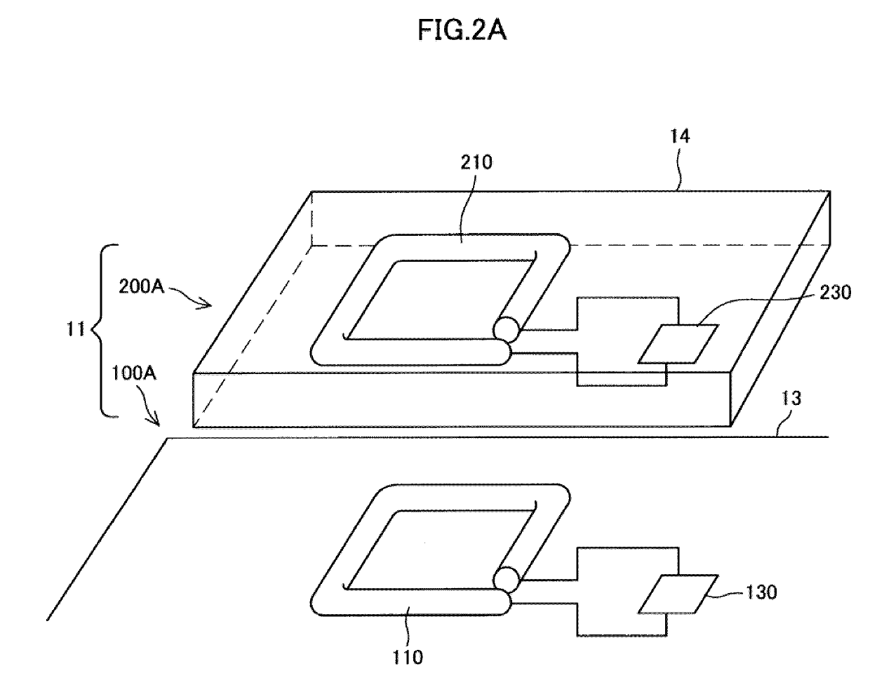
[0098]FIG. 2A is an explanatory diagram illustrating a power transfer device according to a first embodiment of the present invention.

[0099]Of two devices 13 and 14 shown in FIG. 2A, the device 13 on the lower side is a stationary device (for example, a desktop personal computer (PC), a ticket gate machine, a card reader etc.), or a device similar to such stationary devices (for example, a laptop PC etc.). On the other hand, the device 14 on the upper side is a mobile device.

[0100]The devices 13 and 14 include, as a primary circuit 100A or a secondary circuit 200B, the coils (or the loop antennas) 110 and 210 according to each embodiment of the present invention, and the capacitances (not shown in the figures) C1 and C2. In addition, the stationary device 13 on the lower side includes, for example, an electronic circuit 130 that has a power supply circuit and an AC power supply adaptor etc. The device 14 on the upper side includes, for example, an electron...

second embodiment

[0104]Power Transfer Device

[0105]FIG. 2B is an explanatory diagram illustrating a power transfer device according to a second embodiment of the present invention.

[0106]Two devices 14 and 15 shown in FIG. 2B are mobile devices.

[0107]The two devices 15 and 14 respectively include, as a primary circuit 100B and a secondary circuit 200A, the coils (or the loop antennas) 110 and 210 according to each embodiment, of the present invention, and the capacitances (not shown in the figures) C1 and C2. In addition, the two devices 15 and 14 respectively include the electronic circuits 130 and 230 that have, for example, a power supply circuit, a power receiving circuit, and a battery. The two devices 15 and 14 are driven by a battery or the like. The coils, the circuit constants of the power supply circuit and the power receiving circuit, and the like; are set to satisfy the above-described Condition 1 and Condition 2, or Condition 3 and Condition 4. Detailed structures of the coils, the power ...

third embodiment

[0139]Power Transfer Device

[0140]FIG. 8A is a circuit diagram illustrating a power transfer device according to a third embodiment of the present invention. A primary circuit of a power transfer device 21 is illustrated in the lower section of FIG. 8A, and a secondary circuit is illustrated in the upper section. The primary circuit and the secondary circuit are basically formed as described in, for example, the overview of each embodiment of the present invention, but are different in that the primary circuit includes a particular oscillator circuit as a power supply source. Note that, in the following description, the primary circuit is referred to as a power supply device (a power supply device 100C), the secondary circuit (and a tertiary circuit) is referred to as a power receiving device (a power receiving device 200C).

[0141]As shown in FIG. 8A, the power supply device 100C according to the third embodiment, includes the power transfer coil 110, the resonance capacitance (conden...


PUM

PropertyMeasurementUnit
resonance frequencyaaaaaaaaaa
lengthaaaaaaaaaa
lengthaaaaaaaaaa

Abstract

A power transfer device includes: a transformer that couples a primary circuit and a secondary circuit and has a coupling constant of less than 1; and capacitances that are respectively provided in the primary circuit and the secondary circuit, and connected in series with coils that form the transformer. Circuit constants of the primary circuit and the secondary circuit are set so that the primary circuit and the secondary circuit resonate at the same frequency and a product of the square of the coupling constant, a Q value of the primary circuit and a Q value of the secondary circuit is 1. The primary circuit transfers power to the secondary circuit by means of the transformer, using a carrier wave having the resonance frequency.

Description

BACKGROUND OF THE INVENTION[0001]1. Field of the Invention[0002]The present invention relates to a power transfer device, a power supply device and a power receiving device.[0003]2. Description of the Related Art[0004]Recently, various electronic devices have been developed and mobile devices are also widely used. The mobile devices and some stationary devices incorporate batteries as a power source, and the batteries need to be charged by periodically receiving power supplied from the outside. The power supply method used can be roughly classified into, for example, a wired system and a wireless system. In the wired system, for example, a power supply terminal is electrically and directly connected to a terminal of a device to be charged, and power is supplied via this contact point. On the other hand, in the wireless system, for example, a transformer is used, and the device to be charged is electromagnetically coupled to a power supply device in a non-contact manner. Thus, power ...

Claims


Application Information

Patent Timeline
Patent Type & Authority Applications(United States)
IPC IPC(8): H01F38/14
CPCH02J5/005H02J50/12
Inventor IDE, NAOKI
Owner SONY CORP
Why Eureka
Try Eureka