Chemical mechanical polishing aqueous dispersion and chemical mechanical polishing method for semiconductor device

a chemical mechanical and semiconductor technology, applied in the direction of coating machines, nanoinformatics, manufacturing tools, etc., can solve the problems of inability to polish, and inability etc., to achieve the desired thickness, the effect of sufficient and almost equal polishing rates

Inactive Publication Date: 2009-12-31
JSR CORPORATIOON
View PDF16 Cites 17 Cited by
  • Summary
  • Abstract
  • Description
  • Claims
  • Application Information

AI Technical Summary

Benefits of technology

[0011]The chemical mechanical polishing aqueous dispersion according to the invention can polish the polysilicon film, the silicon nitride film, and the silicon oxide film at sufficient and almost equal polishing rates. Therefore, at least two films that form the polishing target surface and are selected from the polysilicon film, the silicon nitride film, and the silicon oxide film can be polished simultaneously. When chemically and mechanically polishing a device having a poly

Problems solved by technology

However, if the polishing rate ratio of the target material to other materials is large, the target material may be polished to a large extent so that defects such as dishing or erosion may occur.
Moreover, since it is necessary to select a chemical mechanical polishing aqueous dispersion corresponding to e

Method used


Image

  • Chemical mechanical polishing aqueous dispersion and chemical mechanical polishing method for semiconductor device
  • Chemical mechanical polishing aqueous dispersion and chemical mechanical polishing method for semiconductor device
  • Chemical mechanical polishing aqueous dispersion and chemical mechanical polishing method for semiconductor device

Examples


examples 1 to 8

3.4 Examples 1 to 8 and Comparative Examples 1 to 10

[0075]In Examples 1 to 8 and Comparative Examples 1 to 10, the component or the concentration of the chemical mechanical polishing aqueous dispersion was changed as shown in Tables 1 and 2. Tables 1 and 2 also show the test results.

[0076]When using the chemical mechanical polishing aqueous dispersions of Examples 1 to 8, the polishing rate ratio of the polysilicon film to the silicon oxide film and the polishing rate ratio of the silicon nitride film to the silicon oxide film were 0.9 to 1.1. The polishing rate of each film was 20 nm / min or more. Specifically, the chemical mechanical polishing aqueous dispersions of Examples 1 to 8 showed a sufficient polishing performance. Therefore, when a semiconductor device having a polishing target surface formed by a polysilicon film, a silicon nitride film, and a silicon oxide film is chemically and mechanically polished by using the chemical mechanical polishing aqueous dispersions of Exam...

first experimental example

3.5.1 First Experimental Example

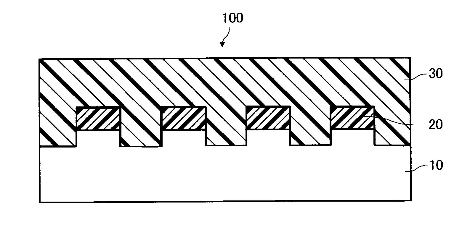
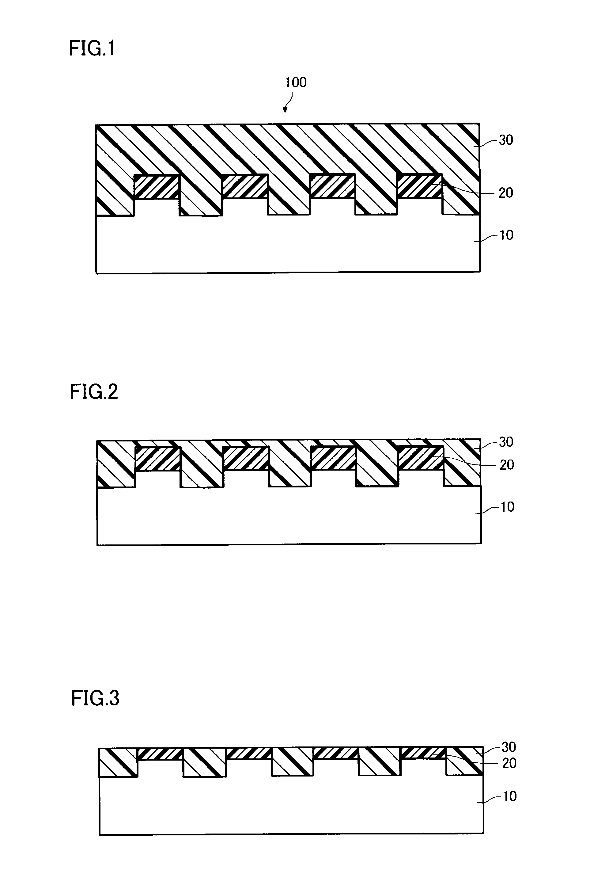
[0088]An evaluation substrate having a polishing target surface formed by a silicon nitride film 20 and a silicon oxide film 30 was provided by preliminarily polishing a commercially available test wafer 100 in which the silicon nitride film 20 was embedded. As the test wafer 100, Sematech 864 (manufactured by Sematech) was used. FIG. 1 is a cross-sectional view showing the test wafer 100. The thickness of the silicon oxide film 30 was 500 nm, and the thickness of the silicon nitride film 20 was 150 nm. The test wafer 100 was preliminarily polished under the following polishing conditions 2 by using CMS4301 and CMS4302 (manufactured by JSR Corporation). Preliminarily polishing was finished in a state in which 50 nm of the silicon oxide film 30 remained on the silicon nitride film 20 to obtain an evaluation substrate, as shown in FIG. 2.

[0089]After preliminarily polishing, the thickness of the silicon oxide film 30 on the silicon nitride film 20 within...

second experimental example

3.5.2 Second Experimental Example

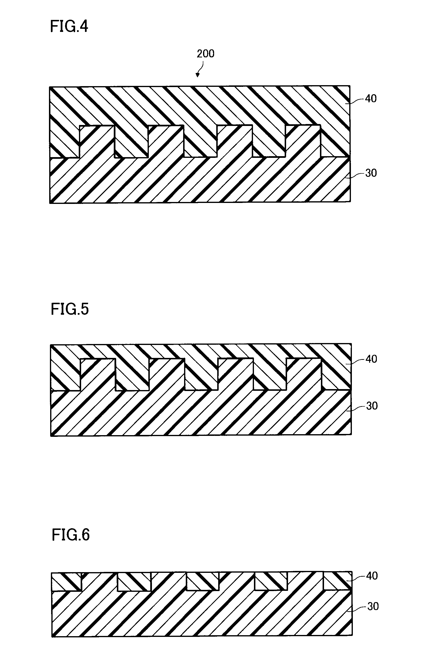
[0092]An evaluation substrate having a polishing target surface formed by a polysilicon film 40 and a silicon oxide film 30 was provided by preliminarily polishing a commercially available test wafer 200 in which the polysilicon film 40 was embedded. As the test wafer 200, SKW3PS (manufactured by SKW) was used. FIG. 4 is a cross-sectional view showing the test wafer 200. The thickness of the polysilicon film 40 was 600 nm, and the thickness of the silicon oxide film 30 was 400 nm. The test wafer 200 was preliminarily polished under the following polishing conditions 3 by using a polysilicon polishing composition. Preliminarily polishing was finished in a state in which 50 nm of the polysilicon film 40 remained on the silicon oxide film 30 in depressions to obtain an evaluation substrate, as shown in FIG. 5.

[0093]After preliminarily polishing, the thickness of the polysilicon film 40 on the silicon oxide film 30 within a 100-micrometer pattern pitch w...


PUM


Abstract

A chemical mechanical polishing aqueous dispersion according to the invention includes (A) 0.1 to 4 mass % of colloidal silica having an average particle diameter of 10 to 100 nm, and (B) 0.1 to 3 mass % of at least one ammonium salt selected from ammonium phosphate, diammonium phosphate, and ammonium hydrogen sulfate, the chemical mechanical polishing aqueous dispersion having a mass ratio (A)/(B) of the component (A) to the component (B) of 1 to 3 and a pH of 4 to 5 and being able to simultaneously polish at least two films that form a polishing target surface and are selected from a polysilicon film, a silicon nitride film, and a silicon oxide film.

Description

TECHNICAL FIELD[0001]The present invention relates to a chemical mechanical polishing aqueous dispersion used when producing a semiconductor device, and a chemical mechanical polishing method using the chemical mechanical polishing aqueous dispersion.BACKGROUND ART[0002]Various materials (e.g., polysilicon film (polycrystalline silicon film), single-crystal silicon film, silicon oxide film, silicon nitride film, aluminum, tungsten, and copper) are normally exposed on a polishing target surface subjected to chemical mechanical polishing (hereinafter may be referred to as “CMP”).[0003]One target material is normally removed by CMP by using a chemical mechanical polishing aqueous dispersion (hereinafter may be referred to as “slurry”) for the target material. However, if the polishing rate ratio of the target material to other materials is large, the target material may be polished to a large extent so that defects such as dishing or erosion may occur. Moreover, since it is necessary t...

Claims


Application Information

Patent Timeline
IPC IPC(8): H01L21/306C09K13/04B24B37/00B82Y10/00H01L21/304
CPCC09G1/02H01L21/3212H01L21/31053B24B37/00H01L21/304
Inventor ANDOU, MICHIAKIKONNO, TOMOHISA
Owner JSR CORPORATIOON
Why Eureka
Try Eureka