System and Method for Conducting Accelerated Soft Error Rate Testing

a technology of soft error rate and test method, which is applied in the field of system and method for conducting accelerated soft error rate test, can solve the problems of overall reliability, soft error rate (ser) of semiconductor devices becoming increasingly important, and susceptibility to error, so as to reduce radiation exposure, improve the effect, and improve the effect of soft error rate of semiconductor devices

Active Publication Date: 2010-01-07
SEMICON MFG INT (SHANGHAI) CORP
View PDF0 Cites 19 Cited by
  • Summary
  • Abstract
  • Description
  • Claims
  • Application Information

AI Technical Summary

Benefits of technology

[0015]The present invention is directed to a system and method for conducting an accelerated soft error rate (ASER) test on semiconductor samples including integrated circuits and semiconductor devices. More particularly, the invention provides for a system and method for carrying out accelerated soft error rate tests with credibility and reliability. The invention provides for a system and method for increasing the effectiveness by which soft error rates of semiconductor devices can be modeled and enhancing by which quality control can be implemented for semiconductor devices. The invention also provides for a system and method of carrying out accelerated soft error rate tests that reduce radiation exposure to an operator of the test. Merely by way of example, the invention can be used to perform testing of BIB or DUT boards in a way compliant with JEDEC standards. Based on the number of soft errors, it may be determined as whether the semiconductor is acceptable. There are other embodiments as well. It would be recognized that the invention has a much broader range of applicability.
[0028]The current invention provides many benefits. According to an embodiment, the invention improves the repeatability and credibility of accelerated soft error rate tests. The proposed tool and method can perform ASER tests at different controlled Geometric Factors (GF's) to help engineers obtain more credible and repeatable relationships between ASER failure rates and radiation stress. According to an embodiment, a GF can be fixed during a test. According to an embodiment a GF can be changed according to a precise and predetermined manner during a test.
[0029]According to an embodiment, a radiation source can be moved during a test such as by disturbances generated by nearby cooling fans. The improved design alleviates such concerns. According to an embodiment, the improved design allows a variety of radiation sources (e.g. alpha-particle and neutron-particle sources) and a variety of semiconductor samples (e.g. silicon wafers and semiconductor chips) to be tested. In addition, the improved tool also allows radiation sources and semiconductor samples of a variety of sizes and shapes to be tested. Some special care in design and manipulations may be required for the extremely small and extremely large radiation sources and semiconductor samples.
[0030]According to an embodiment, the invention enables operators of ASER tests to better control the position and orientation of a radiation source from a DUT board. According to a specific embodiment, the invention allows the distance from die-surface to alpha-particle source as defined in the JEDEC standard to be controlled, facilitating better characterizations of soft error rates in semiconductor devices, which can lead to improved quality control to minimize soft error rates.
[0031]According to another embodiment, the invention also reduces the risk by which operators are subjected to harmful radiation. According to an embodiment, the invention alleviates the need for technicians to hold a radiation source for a prolonged amount of time. This not only improves the quality of test results, but also reduces the risk by which operators are subjected to possibilities of radiation exposure.

Problems solved by technology

As the gate oxide gets thinner and the cell density is increased due to continuous scaling and the rapid technology advancement, however, soft error rates (SER) of semiconductor devices become an increasingly important.
A soft error can be caused by particle strikes including alpha particle strikes and neutron particle strikes.
While an SER is not permanent, it often defines a chip's susceptibility to error and overall reliability.
One of the common causes of SE is particle strikes.
Newer semiconductor chips are becoming increasingly susceptible to SE caused by particle strikes because of the increasing applications of integrated circuits in space where a lot more cosmic rays and particle strikes are expected.
A stray ionizing particles, for example, can generate enough free charge to flip a structure or device to its opposite state, thereby corrupting the operations of a device.
In an integrated circuit (IC) chip package, emission of trace amounts of radioactive impurities is one cause of SEU's.
But in general, even in down-to-earth applications, concerns about soft error rates arising from high density devices means that tests of soft error rates are becoming mandatory in increasingly more and more applications.
A problem with standard ASER tests is the sensitivity the test results depend on the parameters of a test.
The specific distance and orientation at which the technician hold the radiation from the DUT board affect the radiation exposure of the semiconductor device and may thus drastically affect the ASER FIT measurements taken.
A consequence is that test results are often sensitive to the technicians conducting the tests and are difficult to produce with high credibility or reliability.
Another problem with standard ASER tests is the risk technicians are subjected to harmful radiation exposure.
While trained technicians usually handle radiation sources with protective gear, the close proximity by which technicians handle the radiation sources means that technicians can accidentally be subjected to unhealthful doses of harmful radiation in their daily routine.

Method used


Image

  • System and Method for Conducting Accelerated Soft Error Rate Testing
  • System and Method for Conducting Accelerated Soft Error Rate Testing
  • System and Method for Conducting Accelerated Soft Error Rate Testing

Examples


Embodiment Construction

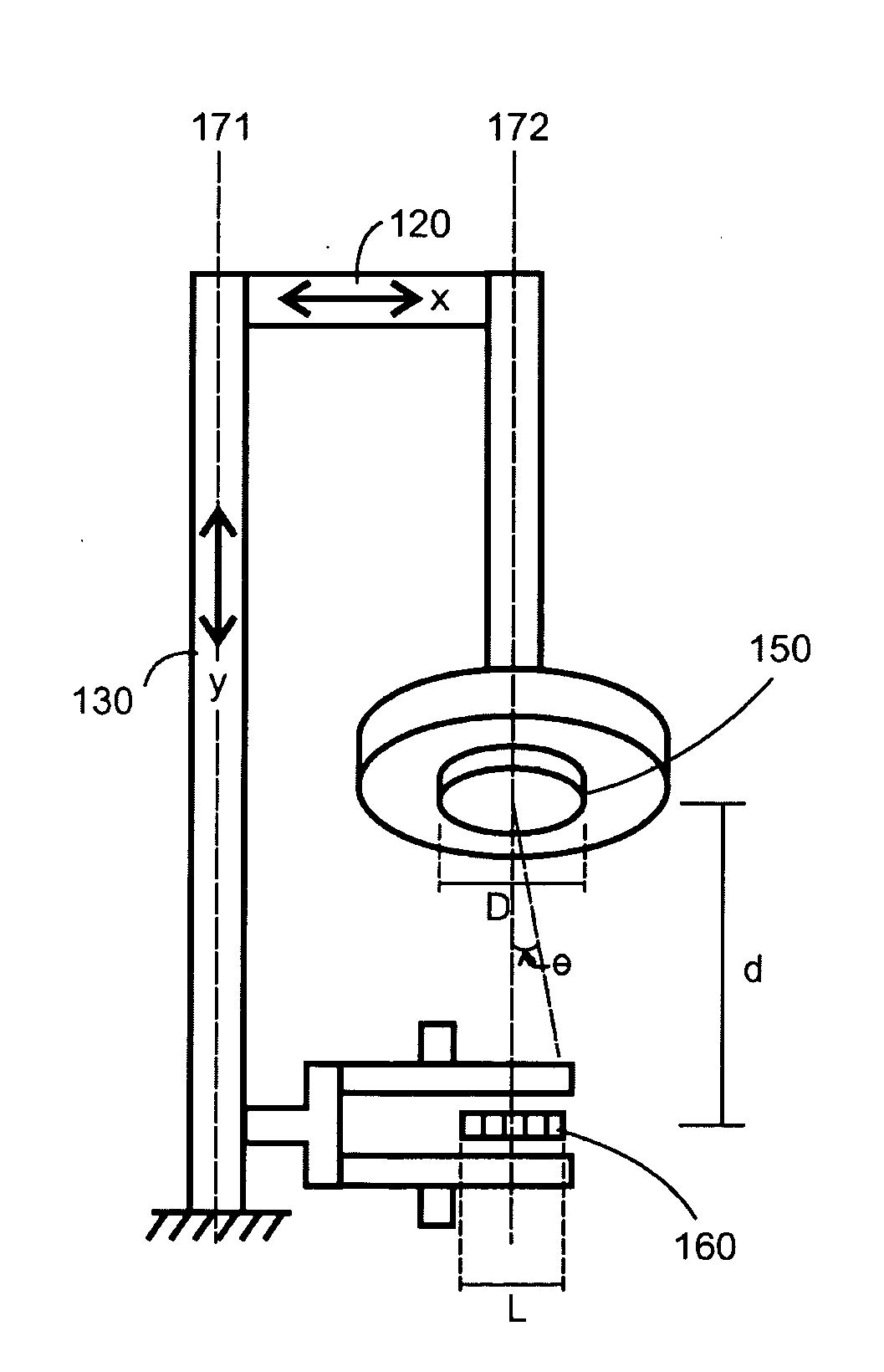
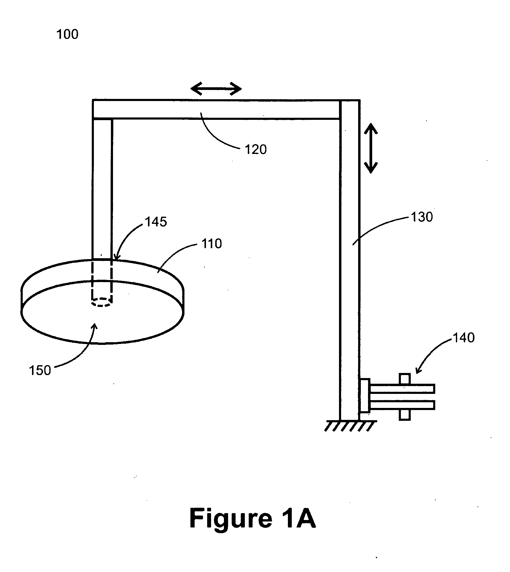
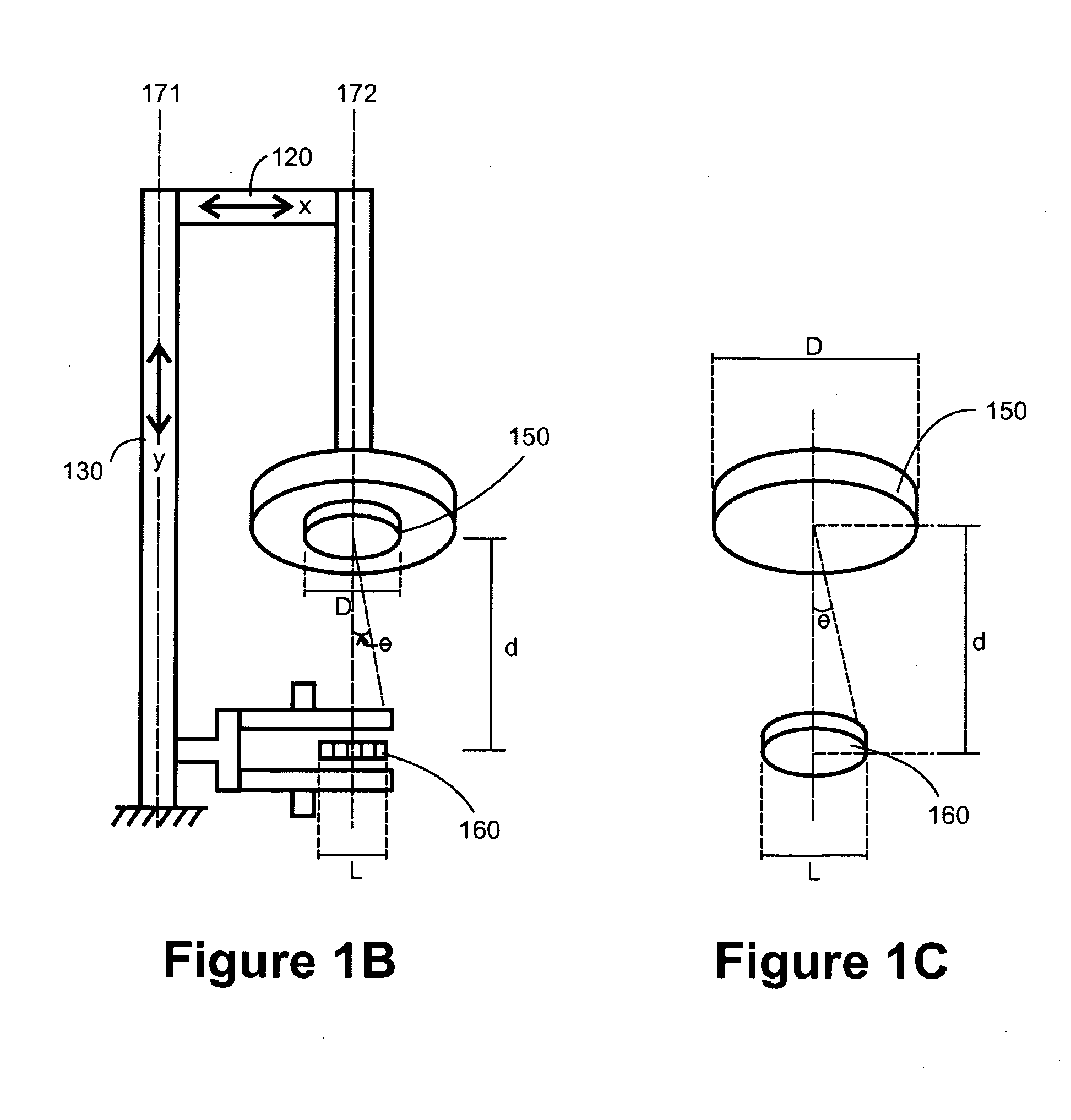
[0056]The present invention is directed to a system and method for conducting an accelerated soft error rate (ASER) test on semiconductor samples including integrated circuits and semiconductor devices. More particularly, the invention provides for a system and method for carrying out accelerated soft error rate tests with credibility and reliability. The invention provides for a system and method for increasing the effectiveness by which soft error rates of semiconductor devices can be modeled and enhancing by which quality control can be implemented for semiconductor devices. The invention also provides for a system and method of carrying out accelerated soft error rate tests that reduce radiation exposure to an operator of the test. Merely by way of example, the invention can be used to perform testing of BIB or DUT boards in a way compliant with JEDEC standards. Based on the number of soft errors, it may be determined as whether the semiconductor is acceptable. There are other e...


PUM


Abstract

An apparatus for a user to conduct an accelerated soft error test (ASER) on a semiconductor sample is provided. The apparatus comprises a first component for holding the radiation source, where the radiation source may be either an alpha-particle or neutron-particle source. The apparatus comprises a second component for holding the semiconductor sample, where the semiconductor sample may be either a silicon wafer or semiconductor chip. The apparatus comprises a connecting assembly for placing the first component and the second component relative to each other at a plurality of positions that subject the semiconductor sample to a radiation stress from the radiation source at a plurality of stress efficiencies. Among the benefits provided are improved repeatability and credibility of ASER tests and reduced radiation exposures to operators of ASER tests.

Description

CROSS-REFERENCES TO RELATED APPLICATIONS[0001]The present application claims the benefit under 35 U.S.C. §119(a) of the following application, the entire disclosures of which, including any attached documents or appendices, are incorporated by reference: Chinese Patent Application No. 200810040292.6, filed Jul. 3, 2008 for “A System and Method for Conducting Accelerated Soft Error Rate Testing” (inventors Jung-Che Chang and Wei-Ting Chien).STATEMENT AS TO RIGHTS TO INVENTIONS MADE UNDER FEDERALLY SPONSORED RESEARCH OR DEVELOPMENT[0002]NOT APPLICABLEREFERENCE TO A “SEQUENCE LISTING,” A TABLE, OR A COMPUTER PROGRAM LISTING APPENDIX SUBMITTED ON A COMPACT DISK[0003]NOT APPLICABLEBACKGROUND OF THE INVENTION[0004]The present invention is directed to a system and method for conducting an accelerated soft error rate (ASER) test on semiconductor samples including integrated circuits and semiconductor devices. More particularly, the invention provides for a system and method for carrying out...

Claims


Application Information

Patent Timeline
Patent Type & Authority Applications(United States)
IPC IPC(8): G01R31/26
CPCG01R31/002G01R31/31816G01R31/2881G01R31/2849
Inventor CHANG, JUNG-CHECHIEN, WEI-TING
Owner SEMICON MFG INT (SHANGHAI) CORP
Why Eureka
Try Eureka