

Nanoscale multi-junction quantum dot device and fabrication method thereof
- Summary
- Abstract
- Description
- Claims
- Application Information
AI Technical Summary
Benefits of technology
Problems solved by technology
Method used
Image

Examples
Embodiment Construction
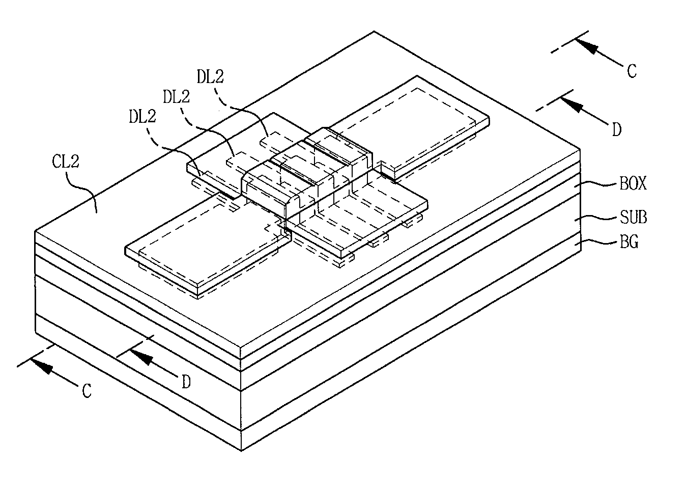
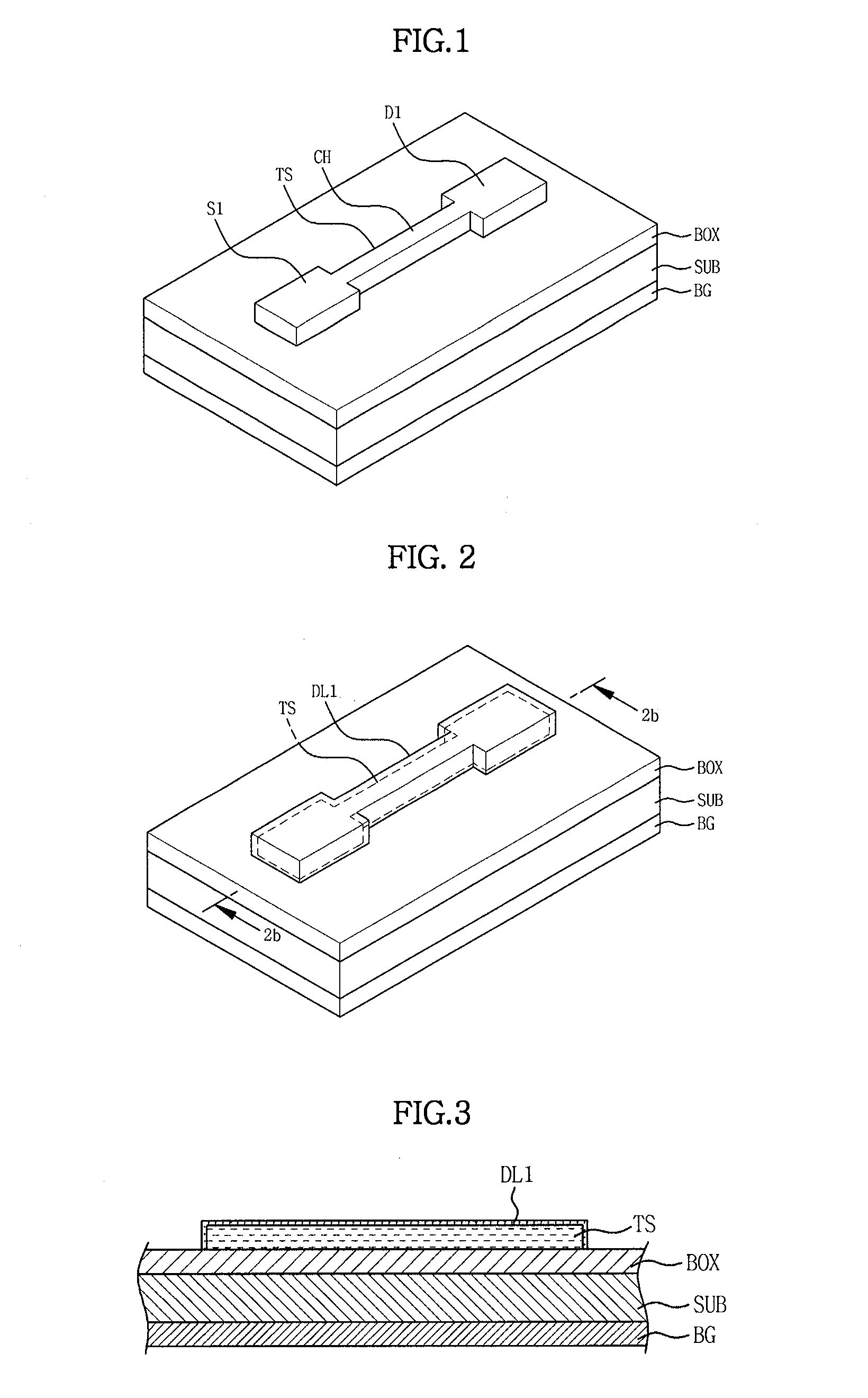
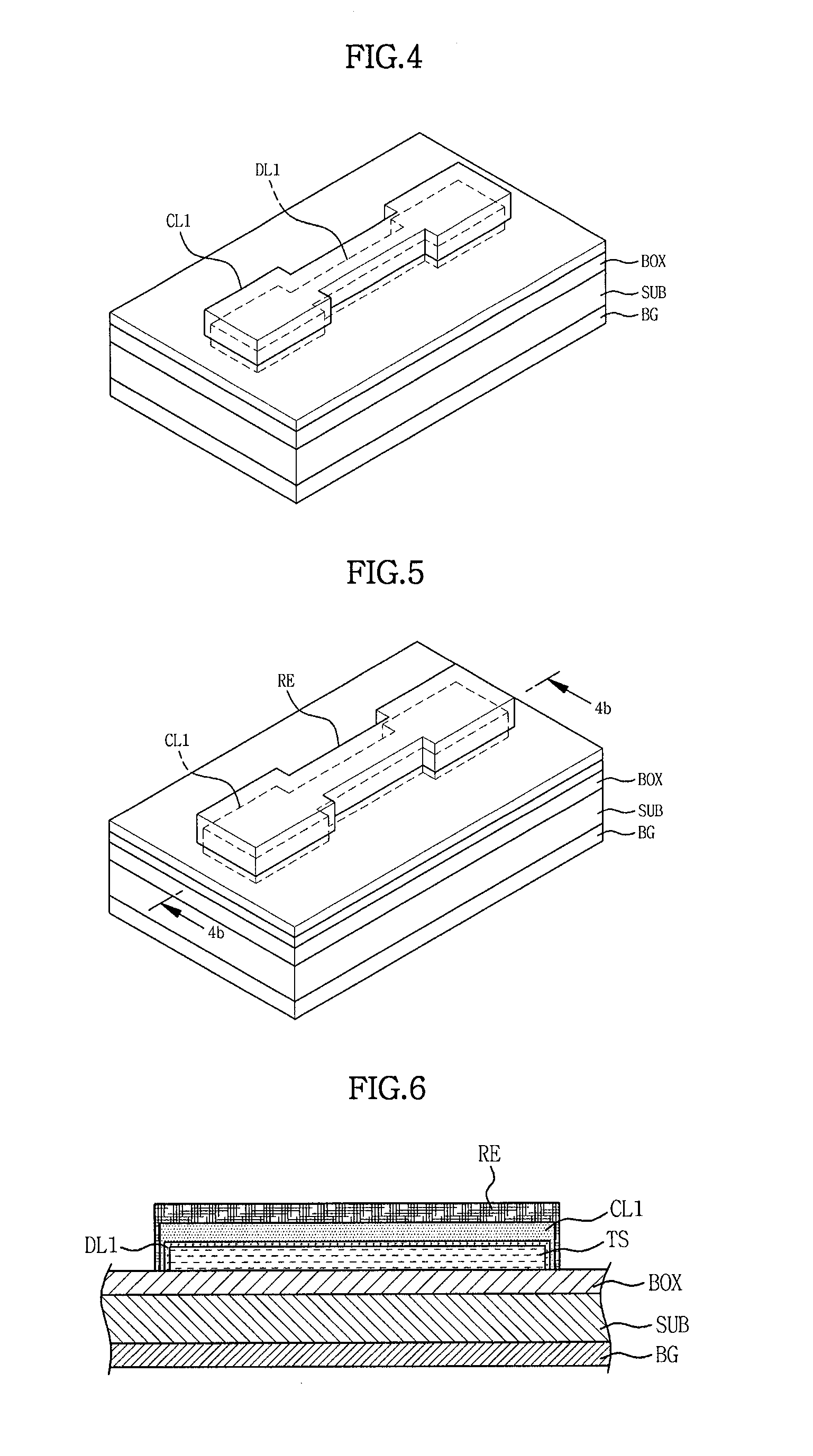
[0084]A method of fabricating a nanoscale multi-junction quantum dot device according to the present invention will now be described with reference to the accompanying drawings.
[0085]Top silicon TS of a wafer first experiences a pattern formation and etch process (a). In a preferred embodiment of the present invention, the wafer has an insulating layer formed between base layers, and may use any kind of a wafer which can increase processing or efficiency of a high-purity silicon layer formed on the insulating layer. However, a Silicon On Insulator (SOI) wafer can be preferably used.
[0086]First, in pattern formation, a pattern is formed so that a source S1 and a drain D1 formed on the top silicon TS at a predetermined interval are connected through a channel CH. In the pattern and etch process, a CMOS process and electron beam lithography are employed so that the channel CH having a line width of several to several tens of nanometers can be formed. The source S1 and the drain D1 resp...
PUM
 Abstract
Description
Claims
Application Information