
Inspection apparatus for inspecting patterns of a substrate

a technology of substrate and inspection apparatus, which is applied in the direction of image analysis, image enhancement, instruments, etc., can solve the problems of difficult to obtain high-resolution images, defects in wiring patterns in stairs, and defects in silicon oxide films or photosensitive photoresist materials through which light is transmitted on the surface cannot be detected, so as to improve inspection efficiency and improve throughput

Inactive Publication Date: 2010-01-14
HITACHI HIGH-TECH CORP
View PDF15 Cites 3 Cited by
  • Summary
  • Abstract
  • Description
  • Claims
  • Application Information

AI Technical Summary

Benefits of technology

The invention is a pattern inspection apparatus and method for inspecting circuit patterns on semiconductor wafers. The apparatus and method improve the efficiency of inspecting by improving the function of a wafer external appearance inspection apparatus. The apparatus can shorten the inspecting time by improving the recipe forming function of the wafer external appearance inspection apparatus, improving ease of use, and improving the inspecting function. The apparatus can also compare different areas of a chip or cells in a cell pitch by designating information of an inspection area and a comparing period. The apparatus can also designate reference image information for each inspection image, which helps in identifying defects on the wafer. The apparatus can also extract inspection and reference images from image data using individual head addresses for each image. The invention also provides an external appearance inspection apparatus that can extract inspection and reference images from image data using position information of the chip or cell in the case of cell comparison or die comparison. The method and apparatus can improve the efficiency of inspecting and shorten the inspecting time by improving the recipe forming function, improving ease of use, and improving the inspecting function.

Problems solved by technology

In the case where the semiconductor wafer in the manufacturing step is inspected by such optical inspection systems as mentioned above, a residual or a defect of the pattern having a silicon oxide film or a photosensitive photoresist material through which light is transmitted on the surface cannot be detected.
Further, a defect occurring in a stairway bottom portion of a wiring pattern cannot be detected.
In the case of the electron beam of a large current and low acceleration, it is difficult to obtain an image of high resolution due to a space-charge effect.
However, in such a type of detection apparatus, since the light emission by phosphor is detected, frequency response characteristics are bad and it is improper to form the electron beam image at a high speed.
An ease of use is bad in both of management and creation of the recipe.
Further, since a plurality of inspection steps are executed every cell, there is such a drawback that the inspecting time becomes long.
However, for example, if a defect is detected in the first chip shown in FIG. 16A, since the one-chip precedent image does not exist and there is no reference image, defect analysis of the first chip is impossible.
Therefore, the reference image includes a larger amount of positional deviation error and a larger amount of error of image concentration or the like and cannot be used as a reference image.
Therefore, even if the defect is detected in the (n+1)th chip in the wafer edge portion, the defect analysis is impossible.
However, since columns of the (n+1)th chip and the nth chip of the chip layouts are different in FIG. 16B, when compared with the relation between the adjacent chips of the same column (for example, the nth chip and the (n−1)th chip), the conditions upon obtaining the images are different and the reference image includes a larger amount of positional deviation error and the like.
Although there is no problem if such an error lies within a correction range of an image processing function, if not, even in the case of FIG. 16B, there is also a possibility that the image of the nth chip cannot be used as a reference image of the (n+1)th chip.
As mentioned above, if the defect is detected in the chip in the semiconductor wafer edge portion and becomes a defect analysis target, since the one-chip precedent image does not exist, the reference image does not exist and a situation that the defect analysis cannot be performed occurs.
However, hitherto, a plurality of cell pitches in the case of the cell comparison cannot be designated.
As mentioned above, according to the related art, since it is necessary to set the cell pitch for each cell pitch area and execute the inspection again, efficiency is very low.
Further, in the die comparison and the cell comparison, since definitions of the reference images which are necessary for the inspection images are different, the cell comparison and the die comparison cannot be mixedly executed.
There is such a drawback that the inspecting time becomes long because a plurality of inspecting steps are repeated.
Further, since a plurality of recipes are needed for one inspection, ease of use is bad in both of the management of the inspection recipes and the creation of the recipes.

Method used


Image

  • Inspection apparatus for inspecting patterns of a substrate
  • Inspection apparatus for inspecting patterns of a substrate
  • Inspection apparatus for inspecting patterns of a substrate

Examples


second embodiment

[0136]the invention will now be described with reference to the drawings.

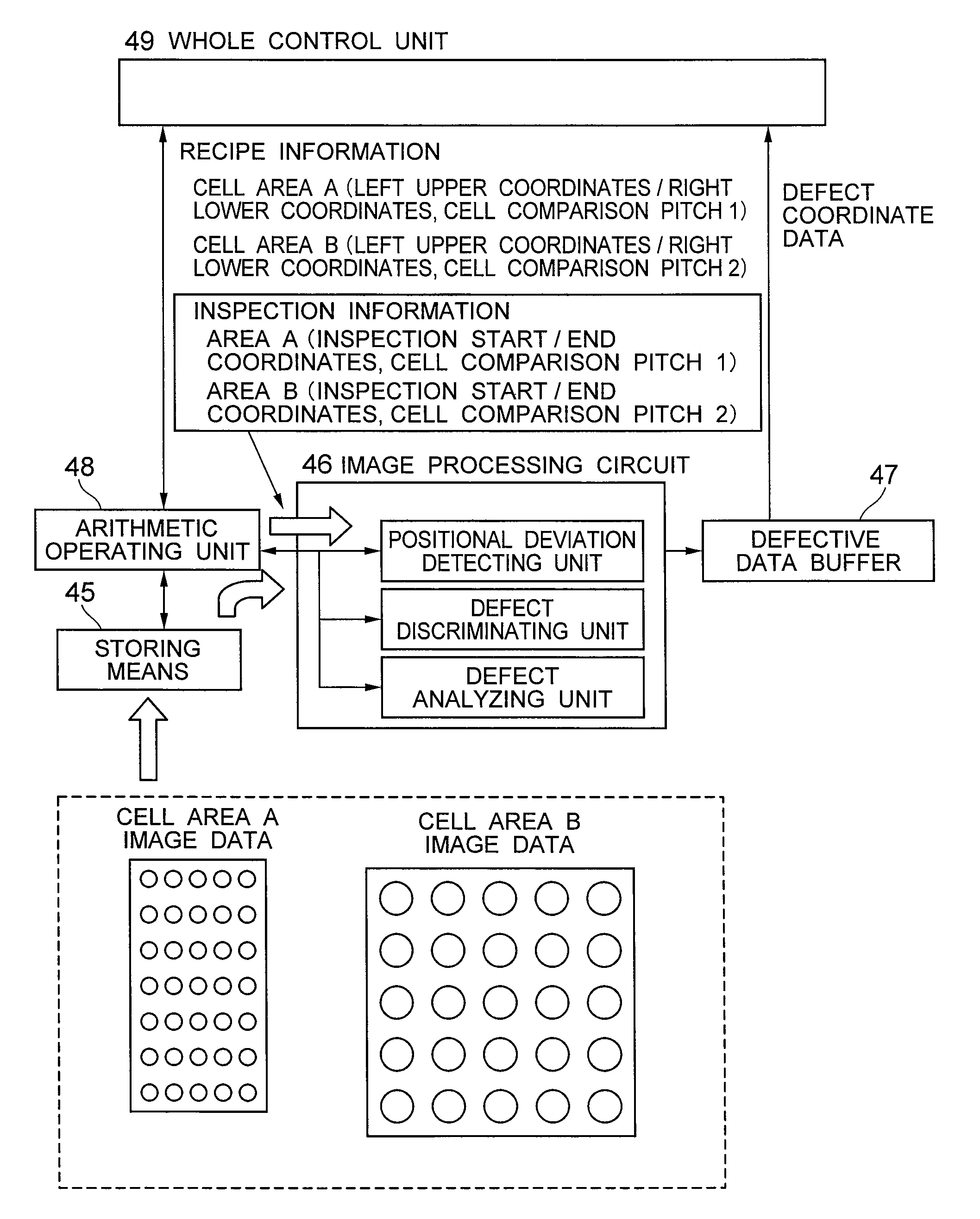
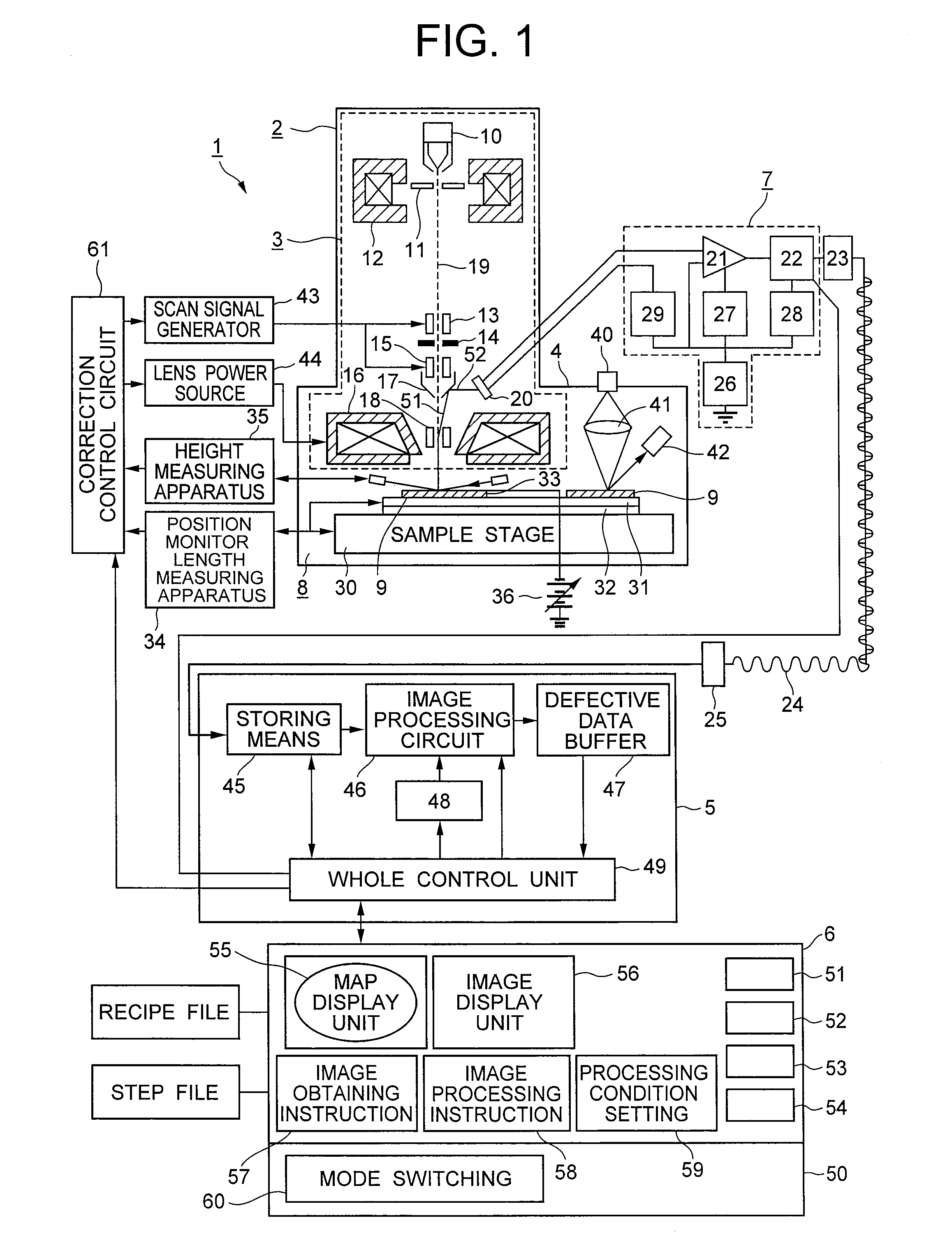
[0137]FIG. 11 is a functional block diagram of an external appearance inspection apparatus of a semiconductor wafer according to the invention. An external appearance of a semiconductor wafer 1100 as an inspection object is photographed by a sensor 1101. The photographed image is converted into digital image data by an A / D converter 1102 and the digital image data is stored into the image memory 1105 of an image processing unit 1103. As functions constructing the image processing unit 1103, besides the image memory 1105, there are the following component elements: a positional deviation detecting unit 1106 to calculate a positional deviation amount between the two image data to be compared; a defect discriminating unit 1107 to obtain a differential image between the two images by using the positional deviation amount calculated by the positional deviation detecting unit and extract defect candidates from the di...

third embodiment

[0168]the invention will now be described.

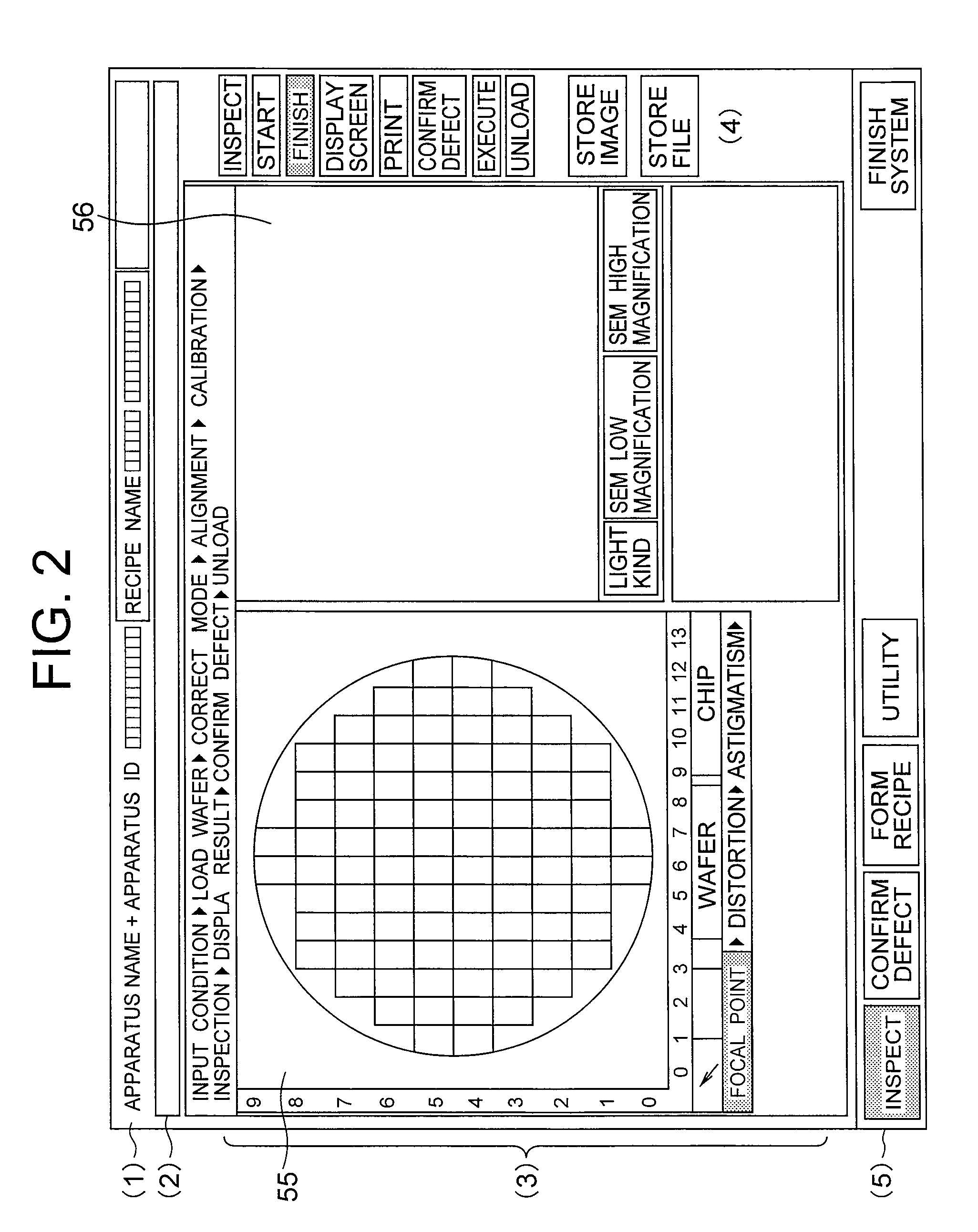
[0169]The inspection threshold value will now be described with respect to the memory cell area as an example with reference to FIG. 24. As shown in FIG. 24, the same pattern is periodically repeated in the memory cell areas in the chip. The images are compared in accordance with such a repetitive period and the pattern in which the brightness, size, or the like of the image is equal to or larger than a specific value which is determined by the user designation or the like is determined to be a defect. Such a specific value as a comparing condition is called an inspection threshold value. There is a case where a plurality of memory cell areas of different cell pitches exist in the chip. In this case, since the degrees of the brightness of the memory cell areas differ, if the comparison inspection is executed by the inspection threshold value 1 in the memory cell area A and the comparison inspection is executed by the inspection threshold val...


PUM


Abstract

A pattern inspection apparatus has a setting unit of a plurality of cell areas A and B of different cell comparison pitches and inspects the plurality of cell areas of the different cell comparison pitches in accordance with settings of the setting unit. As information to read out image data for an inspection image and a reference image from an image memory, in addition to position information of a defective image, identification information showing either a cell comparison or a die comparison and relative position information of the reference image can be set. The apparatus also has a unit for setting a plurality of inspection threshold values every inspection area and inspects a plurality of inspection areas by the plurality of inspection threshold values.

Description

RELATED APPLICATIONS[0001]This application is a Divisional of U.S. patent application Ser. No. 11 / 344,101, filed on Feb. 1, 2006, claiming priority of Japanese Patent Application Nos. 2005-025480, filed on Feb. 1, 2005, 2005-067664, filed on Mar. 10, 2005, and 2005-251237, filed on Aug. 31, 2005, the entire contents of each of which are hereby incorporated by reference.BACKGROUND OF THE INVENTION[0002]The invention relates to a pattern inspection apparatus of a substrate having a fine circuit pattern like a semiconductor device, liquid crystal, or the like and, more particularly, to a pattern inspection apparatus which is suitable when it is applied to a pattern inspection on a wafer during a semiconductor device manufacturing step.[0003]An inspection of a semiconductor wafer will be described as an example. A semiconductor device is manufactured by repeating a step of transferring a pattern formed on a photomask onto the semiconductor wafer by a lithography process and an etching p...

Claims


Application Information

Patent Timeline
Patent Type & Authority Applications(United States)
IPC IPC(8): G06K9/00
CPCG06T2207/30148G06T7/001
Inventor HAYAKAWA, KOICHIMIYAI, HIROSHINOJIRI, MASAAKINAKANO, MICHIOFUJISAWA, TAKAKOFUJII, DAI
Owner HITACHI HIGH-TECH CORP
Learn More