Transparent conductive film, transparent conductive laminate, touch panel, and method for producing transparent conductive film

Active Publication Date: 2010-01-21
NITTO DENKO CORP
View PDF11 Cites 82 Cited by
  • Summary
  • Abstract
  • Description
  • Claims
  • Application Information

AI Technical Summary

Benefits of technology

[0019]In the above, it is preferable that the first transparent dielectric layer, the second transparent dielectric layer and the transparent conductive layer are formed on both sides of the transparent film substrate, and it further comprises a transparent substrate placed on a side of one of the transparent conductive layers opposite to the second transparent dielectric layer. Also in this case, the mechanical strength of the film can be improved, and in particular, curling or the like can be prevented.
[0020]The transparent conductive film of the invention is suitable for use in touch panels based on various detection methods (such as capacitive types and resistive film types) and particularly suitable for use in capacitive touch panels. Capacitive touch panels have a patterned transparent conductive layer formed over the surface of the display unit. In such capacitive tough panels, therefore, the function according to the invention (the function of reducing the difference in reflectance between the pattern portion and the portion immediately below the pattern opening portion) is more effectively performed.
[0021]Also, the transparent conductive laminate of the present invention is a transparent conductive laminate, comprising two or more transparent conductive films laminated with a transparent pressure-sensitive adhesive layer interposed therebetween, wherein at least one of the transparent conductive films is the above transparent conductive film of the invention, and the transparent conductive layer of the transparent conductive film is placed on at le

Problems solved by technology

In the transparent conductive film described in Japanese Patent Application Laid-Open (JP-A) No. 2008-98169, however, the difference between th

Method used


Image

  • Transparent conductive film, transparent conductive laminate, touch panel, and method for producing transparent conductive film
  • Transparent conductive film, transparent conductive laminate, touch panel, and method for producing transparent conductive film
  • Transparent conductive film, transparent conductive laminate, touch panel, and method for producing transparent conductive film

Examples


first embodiment

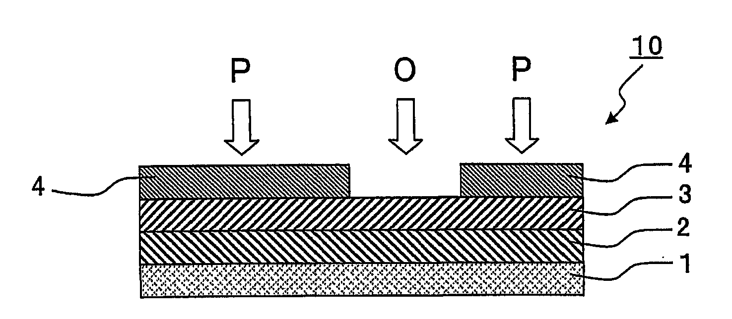
[0037]FIG. 1 is a cross-sectional view of a transparent conductive film according to a first embodiment of the invention. Referring to FIG. 1, the transparent conductive film 10 includes a transparent film substrate 1 and a first transparent dielectric layer 2, a second transparent dielectric layer 3 and a transparent conductive layer 4 that are sequentially formed on one side of the transparent film substrate 1. The transparent conductive layer 4 is patterned to form a pattern portion P and a pattern opening portion O.

[0038]The transparent conductive film 10 satisfies the relation n231, wherein n1, n2 and n3 are the refractive indices of the first transparent dielectric layer 2, the second transparent dielectric layer 3 and the transparent conductive layer 4, respectively. The first transparent dielectric layer 2 has a thickness of from 2 nm to less than 10 nm (preferably from 2 to 9 nm, more preferably from 3 to 8 nm). The second transparent dielectric layer 3 has a thickness of f...

second embodiment

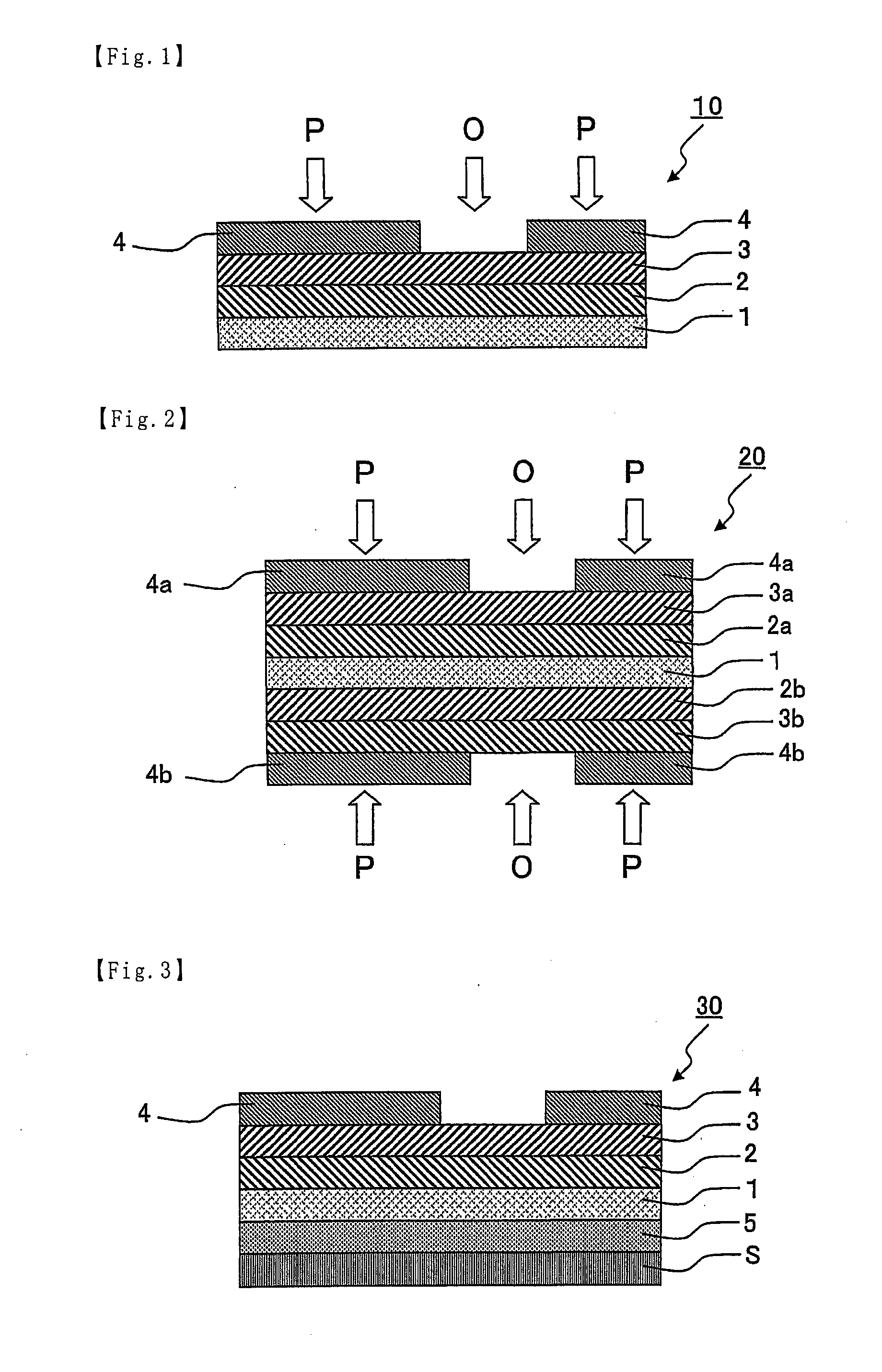
[0056]Next, a description is given of a transparent conductive film according to a second embodiment of the invention. FIG. 2 is a cross-sectional view of the transparent conductive film according to the second embodiment of the invention. Referring to FIG. 2, the transparent conductive film 20 includes a transparent film substrate 1 and a first transparent dielectric layer 2a, a second transparent dielectric layer 3a and a transparent conductive layer 4a that are sequentially formed on the upper side of the transparent film substrate 1, and another first transparent dielectric layer 2b, another second transparent dielectric layer 3b and another transparent conductive layer 4b that are sequentially formed on the lower side of the transparent film substrate 1. The transparent conductive layers 4a and 4b are each patterned to form a pattern portion P and a pattern opening portion O.

[0057]The transparent conductive film 20 satisfies the relation n2a3a1a, wherein n1a, n2a and n3a are th...

third embodiment

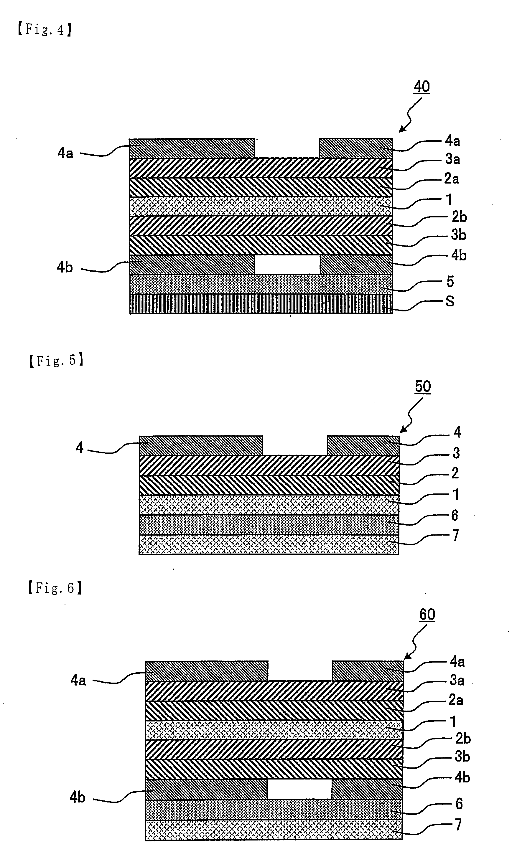
[0060]Next, a description is given of a transparent conductive film according to a third embodiment of the invention. FIG. 3 is a cross-sectional view of the transparent conductive film according to the third embodiment of the invention. Referring to FIG. 3, the transparent conductive film 30 includes the structure of the transparent conductive film 10 described above and a separator S placed on the lower side of the transparent film substrate 1 with a transparent pressure-sensitive adhesive layer 5 interposed therebetween.

[0061]Any transparent pressure-sensitive adhesive may be used for the transparent pressure-sensitive adhesive layer 5 without limitation. For example, the pressure-sensitive adhesive may be appropriately selected from transparent adhesives based on polymers such as acrylic polymers, silicone polymers, polyester, polyurethane, polyamide, polyvinyl ether, vinyl acetate-vinyl chloride copolymers, modified polyolefins, epoxy polymers, fluoropolymers, and rubbers such ...


PUM

PropertyMeasurementUnit
Percent by massaaaaaaaaaa

Abstract

The transparent conductive film of the present invention is a transparent conductive film, comprising a transparent film substrate, and a first transparent dielectric layer, a second transparent dielectric layer and a transparent conductive layer that are formed on one or both sides of the transparent film substrate in this order from the transparent film substrate side, wherein the transparent conductive layer is patterned, the relation n2<n3<n1 is satisfied, wherein n1 is the refractive index of the first transparent dielectric layer, n2 is the refractive index of the second transparent dielectric layer, and n3 is the refractive index of the transparent conductive layer, the first transparent dielectric layer has a thickness of from 2 nm to less than 10 nm, the second transparent dielectric layer has a thickness of from 20 nm to 55 nm, and the transparent conductive layer has a thickness of from 15 nm to 30 nm.

Description

BACKGROUND OF THE INVENTION[0001]1. Field of the Invention[0002]The invention relates to a transparent conductive film, a transparent conductive laminate therewith, a touch panel therewith, and a method for producing a transparent conductive film.[0003]2. Description of the Related Art[0004]Concerning conventional transparent conductive components, the so-called conductive glass is well known, which includes a glass member and an indium oxide thin film formed thereon. Since the base member of the conductive glass is made of glass, however, it has low flexibility or workability and cannot preferably be used in some applications. In recent years, therefore, transparent conductive films using various types of plastic films such as polyethylene terephthalate films as their substrates have been used, because of their advantages such as good impact resistance and light weight as well as flexibility and workability.[0005]A known transparent conductive film for detecting input positions inc...

Claims


Application Information

Patent Timeline
IPC IPC(8): G06F3/041B32B17/00B32B3/10
CPCC23C14/08G06F3/041Y10T428/2495Y10T428/24802Y10T428/24967Y10T428/24942Y10T428/24926G06F3/044G06F3/0412G06F3/045H01B5/14G06F2203/04103
Inventor NASHIKI, TOMOTAKENAKAJIMA, KAZUHIROSUGAWARA, HIDEO
Owner NITTO DENKO CORP
Why Eureka
Try Eureka