Semiconductor light-emitting device

a technology of semiconductor devices and light-emitting devices, which is applied in the direction of semiconductor devices, lasers, semiconductor lasers, etc., can solve the problems putting current leakage into an nonnegligible situation, and achieve the effect of increasing current leakag

Active Publication Date: 2010-01-28
SONY CORP
View PDF28 Cites 7 Cited by
  • Summary
  • Abstract
  • Description
  • Claims
  • Application Information

AI Technical Summary

Benefits of technology

[0248]the sixth compound semiconductor layer is in contact with the side of the first compound semiconductor layer (at least a portion of the side of the first A compound semiconductor layer and the whole side of the first b compound semiconductor layer), and the third compound semiconductor layer is in contact with the side of the second compound semiconductor layer. By employing this structure, the first B compound semiconductor layer and the fourth compound semiconductor layer which have uncompetitive impurity substitute sites are not in contact with each other, and thus impurity diffusion can be prevented. In this case, an alternative route includes the first compound semiconductor layer (the first A compound semiconductor layer and the first B compound semiconductor layer), the sixth compound semiconductor layer, the fourth compound semiconductor layer, the third compound semiconductor layer, and the second compound semiconductor layer, and the pn junction interfaces include the three interfaces of the sixth compound semiconductor layer / the fourth compound semiconductor layer, the fourth compound semiconductor layer / the third compound semiconductor layer, and the third compound semiconductor layer / the side of the second compound semiconductor layer.
[0395]The semiconductor light-emitting device according to each of the ninth, eleventh, thirteenth, and fifteenth embodiments of the present invention has the third compound semiconductor layer including at least three layers or the fourth compound semiconductor layer including at least three layers, and the third B compound semiconductor layer or the fourth B compound semiconductor layer in contact with a side of the active layer contains carbon (C) or silicon (Si) which is the impurity with relatively low diffusibility. Therefore, impurity diffusion into the active layer from the compound semiconductor layer in contact with a side of the active layer can be decreased. On the other hand, the semiconductor light-emitting device according to each of the tenth, twelfth, fourteenth, and sixteenth embodiments of the present invention has the third compound semiconductor layer or the fourth compound semiconductor layer which is composed of a compound semiconductor layer co-doped with carbon (C) or silicon (Si) which is an impurity with relatively low diffusibility. Therefore, impurity diffusion into the active layer from the compound semiconductor layer in contact with a side of the active layer can be decreased.

Problems solved by technology

In particular, in the {hll}B crystal plane region or the vicinity thereof, there occurs the problem that the current-blocking layer disappears or decreases in thickness due to impurity inter-diffusion between a n-type compound semiconductor layer and a p-type compound semiconductor layer which constitute the current-blocking layer, and thus the effect of the current-blocking layer is not stabilized, thereby increasing a current leakage.
In addition, when the SDH-type semiconductor laser is driven with a high driving current, a current leakage is being put into an nonnegligible situation due to impurities which diffuse into the active layer from the current-blocking layer.

Method used


Image

  • Semiconductor light-emitting device
  • Semiconductor light-emitting device
  • Semiconductor light-emitting device

Examples


example 1

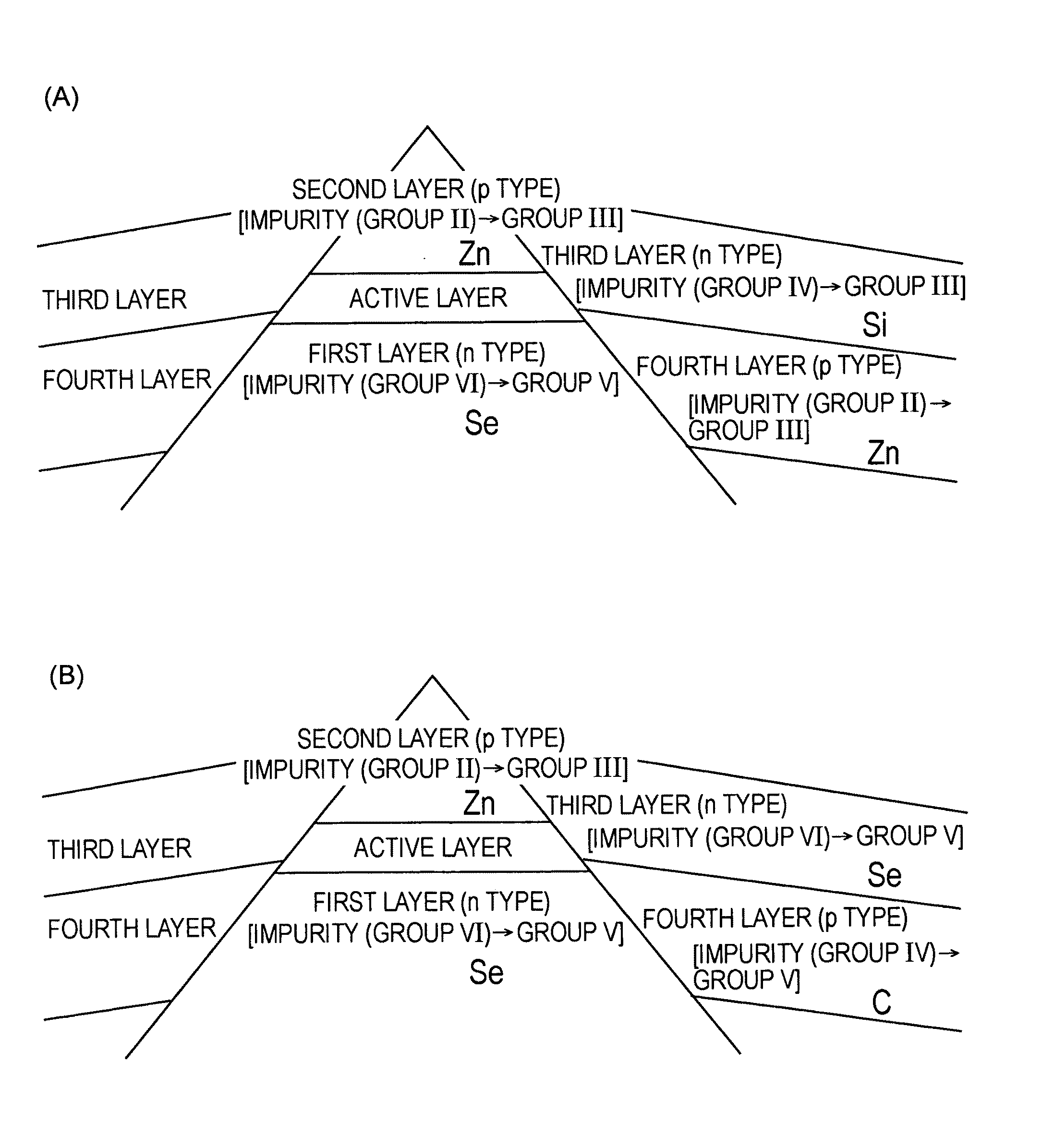
[0427]Example 1 relates to semiconductor light-emitting devices according to a first embodiment of the present invention (more specifically, an embodiment 1-A-1), a second embodiment of the present invention (more specifically, an embodiment 2-A), and a fourth embodiment of the present invention.

[0428]In Example 1 or Examples 2 to 25 described below, at least one type of impurity (group VI impurity) selected from the group consisting of selenium (Se), tellurium (Te), and sulfur (S), specifically selenium (Se), is used, at least one type of impurity (group IV impurity) selected from the group consisting of silicon (Si) and tin (Sn), specifically silicon (Si), is used, and at least one type of impurity (group II impurity) selected from the group consisting of zinc (Zn), magnesium (Mg), beryllium (Be), and manganese (Mn), specifically zinc (Zn), is used. However, impurities are not limited to these.

[0429]In addition, each of the semiconductor light-emitting devices in Example 1 or Exam...

example 2

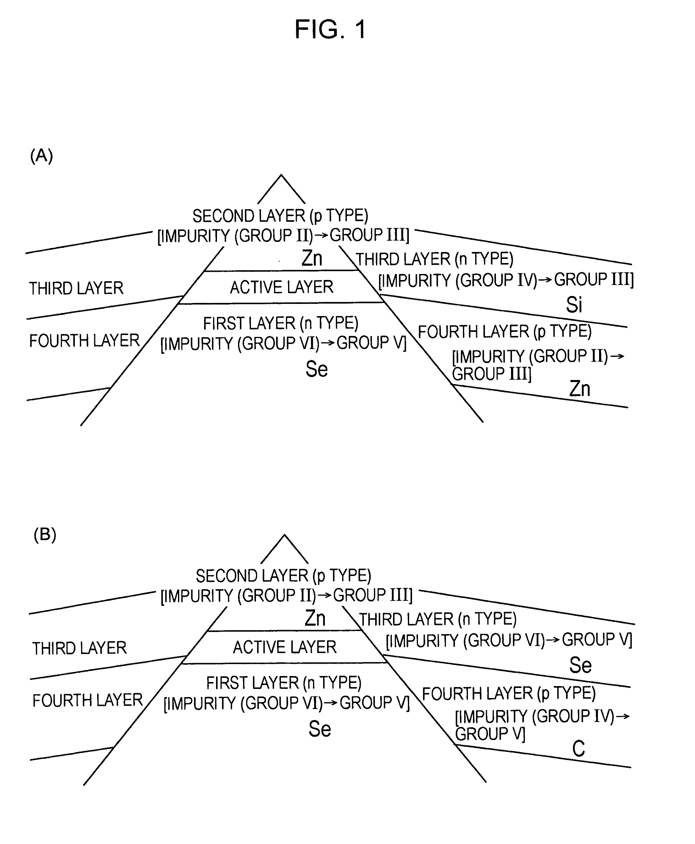
[0510]Example 2 is a modification of Example 1 and relates to an embodiment 1-B-1 of the present invention and an embodiment 2-B of the present invention.

[0511]Specifically, as shown in a conceptual view of FIG. 4(A), when a semiconductor light-emitting device of Example 2 is described with reference to the embodiment 1-B-1 of the present invention,

[0512]a first compound semiconductor layer, a second compound semiconductor layer, a third compound semiconductor layer, and a fourth compound semiconductor layer are composed of group III-V compound semiconductors,

[0513]the first compound semiconductor layer includes a first A compound semiconductor layer and a first B compound semiconductor layer provided on the first A compound semiconductor layer so as to be in contact with an active layer,

[0514]the second compound semiconductor layer includes a second B compound semiconductor layer in contact with the active layer and a second A compound semiconductor layer provided on the second B c...

example 3

[0531]Example 3 is also a modification of Example 1 and relates to an embodiment 1-C-1 of the present invention and an embodiment 2-C of the present invention and further relates to a six embodiment of the present invention. In Example 3 or Example 4 described below, the conductivity types are opposite to those in Example 1. Namely, in Example 3 or Example 4 described below, the first conductivity type is p-type, and the second conductivity type is n-type.

[0532]Specifically, as shown in a conceptual view of FIG. 7(A), a schematic partial sectional view of FIG. 29(A), and an enlarged schematic partial sectional view of FIG. 29(B), when a semiconductor light-emitting device of Example 3 is described with reference to the embodiment 1-C-1 of the present invention,

[0533]a first compound semiconductor layer 21, second compound semiconductor layers 22A and 22B, and a current-blocking layer 40 (a third compound semiconductor layer 43 and a fourth compound semiconductor layer 44) are compos...


PUM


Abstract

There is provided a semiconductor light-emitting device capable of an attempt to further decrease a leakage current in a current-blocking layer and including (A) a light-emitting portion (20) composed of a first compound semiconductor layer (abbreviated as a layer hereinafter) (21) having a first conductivity type, an active layer (23), and a second layer (22) having a second conductivity type, and (B) a current-blocking layer (40) in contact with the side of the light-emitting portion and composed of a third layer (43) having the first conductivity type and a fourth layer (44) having the second conductivity type, wherein the impurity for imparting the first conductivity type to the first layer (21) includes an impurity in the first layer (21) at a substitution site which is uncompetitive with a substitution site of the impurity in the second layer (22), for imparting the second conductivity type to the second layer (22), and the impurity for imparting the first conductivity type to the third layer (43) includes an impurity in the third layer (43) at a substitution site which is competitive with a substitution site of the impurity in the fourth layer (44), for imparting the second conductivity type to the fourth layer (44).

Description

TECHNICAL FIELD[0001]The present invention relates to a semiconductor light-emitting device and more specifically to a semiconductor light-emitting device including a current-blocking layer provided in a light-emitting portion in a lateral direction thereof, for narrowing a current.BACKGROUND ART[0002]A semiconductor laser (referred to as a “SDH-type semiconductor laser” hereinafter) having a SDH (Separated Double Hetero Junction) structure which can be formed by one time of an epitaxial growth process is known as a semiconductor layer having low threshold current Ith, for example, from U.S. Pat. No. 2,990,837.[0003]In this SDH-type semiconductor laser, first, a projecting portion is formed on a substrate having a {100} plane as a main surface to extend in the direction of a {110}A plane. In crystal growth on the main surface of the substrate, a light-emitting portion composed of a laminated structure of compound semiconductor layers is formed on the {100} plane of the projecting po...

Claims


Application Information

Patent Timeline
Patent Type & Authority Applications(United States)
IPC IPC(8): H01L33/00H01S5/227H01S5/343
CPCB82Y20/00H01L33/145H01S5/2201H01S5/2222H01S5/2223H01S5/3432H01S5/305H01S5/3054H01S5/3072H01S5/3077H01S5/3211H01S5/227H01L33/18
Inventor KARINO, SACHIOTAKASE, EIJIOOGANE, MAKOTONAGATAKE, TSUYOSHIKAMADA, MICHIRUNARUI, HIRONOBUOKANO, NOBUKATA
Owner SONY CORP
Why Eureka
Try Eureka