Surface emitting laser

a surface emitting laser and laser technology, applied in semiconductor lasers, laser details, electrical equipment, etc., can solve problems such as degrading device characteristics, problem with current injection, and /2 micro-cavity surface emitting lasers, and achieve low-threshold, high-efficiency device characteristics, and light intensity increase

Inactive Publication Date: 2010-01-28
NEC CORP
View PDF0 Cites 12 Cited by
  • Summary
  • Abstract
  • Description
  • Claims
  • Application Information

AI Technical Summary

Benefits of technology

[0021]It is an object of the present invention to provide a surface emitting laser which is capable of achieving a low threshold, a high efficiency, and a high-speed modulation in a micro-cavity structure which includes an optical resonator unit which has an optical path length approximate to λ / 2.
[0023]According to the present invention, light intensity can be increased in an active layer in a micro-cavity structure which includes an optical resonator unit having an optical path length close to λ / 2, thus attaining low-threshold, highly efficient device characteristics. Also, current can be readily injected into the active layer to increase the injection current, increase the relaxation oscillation frequency, and improve high-speed modulation performance.

Problems solved by technology

However, the λ / 2 micro-cavity surface emitting laser described in the aforementioned document has a problem with respect to current injection.
However, if they are applied to the optical resonator unit, the device characteristics are degraded because optical absorption increases, and a large electric field is applied to the active layer.
Accordingly, even if an attempt is made to inject a current into such a structure, low refraction index layer 2123, which corresponds to the large band gap layer, serves as a current block layer, thus making it difficult to inject a current into the active layer.

Method used


Image

  • Surface emitting laser
  • Surface emitting laser
  • Surface emitting laser

Examples


example 1

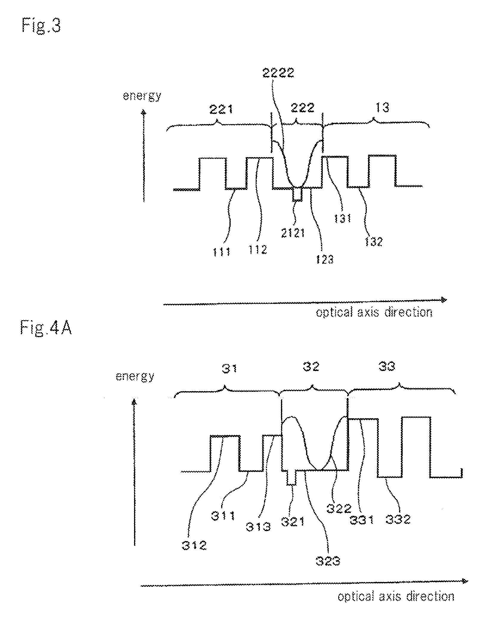
[0105]FIG. 4A is a diagram showing a band structure and an electric field strength curve of a surface emitting laser according to this Example. The configuration of the surface emitting laser of this Example will be described with reference to FIG. 4A.

[0106]The surface emitting laser of this Example comprises first multilayer Bragg reflecting mirror 31 comprised of a semiconductor material, second multilayer Bragg reflecting mirror 33 comprised of a dielectric material, and optical resonator unit 32 sandwiched by these DBRs. First multilayer Bragg reflecting mirror 31 corresponds to a semiconductor DBR. Second multilayer Bragg reflecting mirror 33 corresponds to a dielectric DBR.

[0107]First multilayer Bragg reflecting mirror 31 comprises alternating multiple layers of first low refraction index layer 312 and first high refraction index layer 311, each of which has a thickness of λ / 4. Second multilayer Bragg reflecting mirror 33 comprises alternating multiple layers of second low ref...

example 2

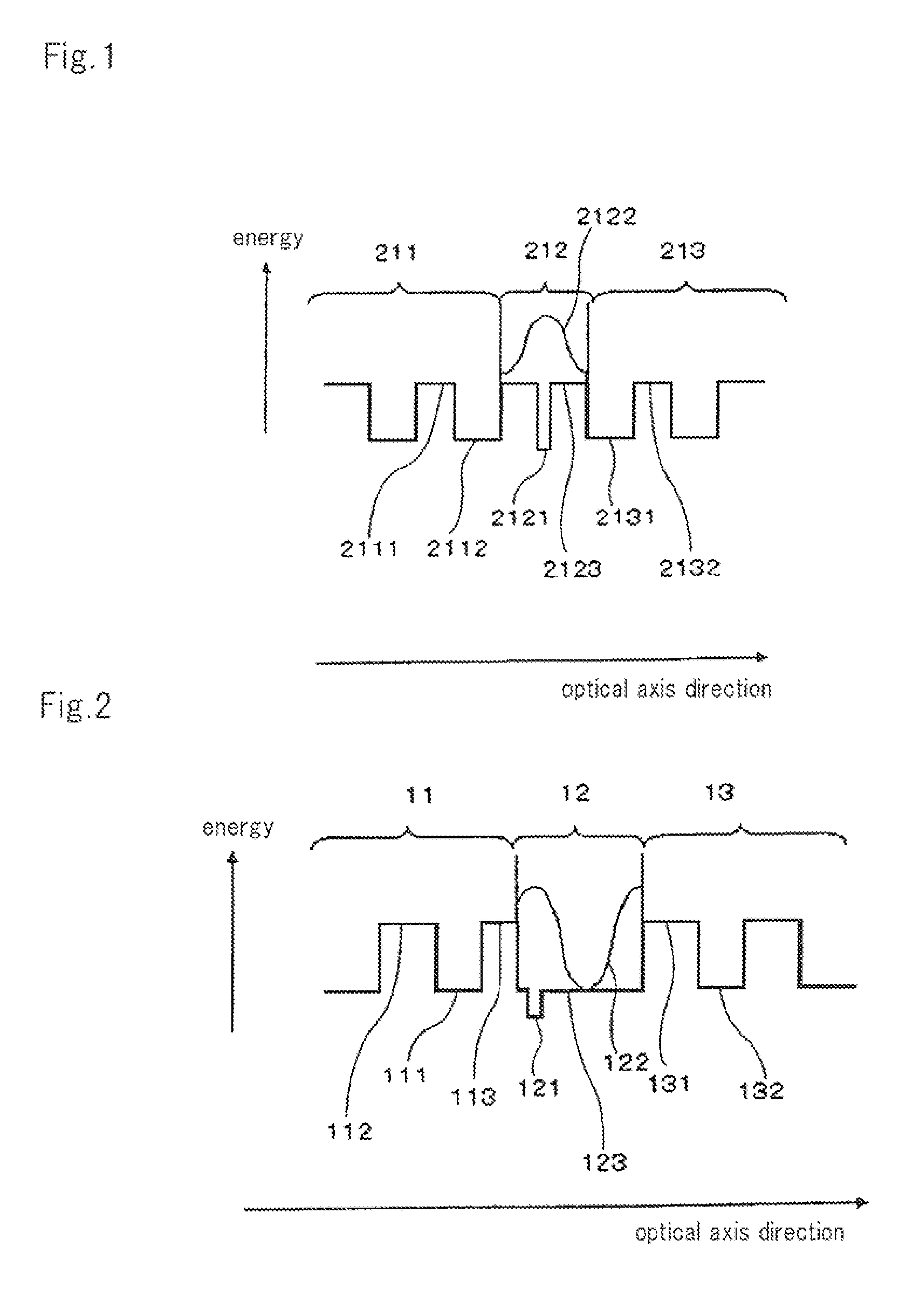
[0121]In this Example, a description will be given of an exemplary configuration of a current injection type VCSEL structure. FIG. 6A is a schematic diagram showing a band structure of a surface emitting laser according to this Example, and FIG. 6B is a schematic diagram showing a cross-section of the device structure. While FIG. 6A does not show the vertical axis or horizontal axis, the vertical axis and horizontal axis are similar to those in FIG. 2.

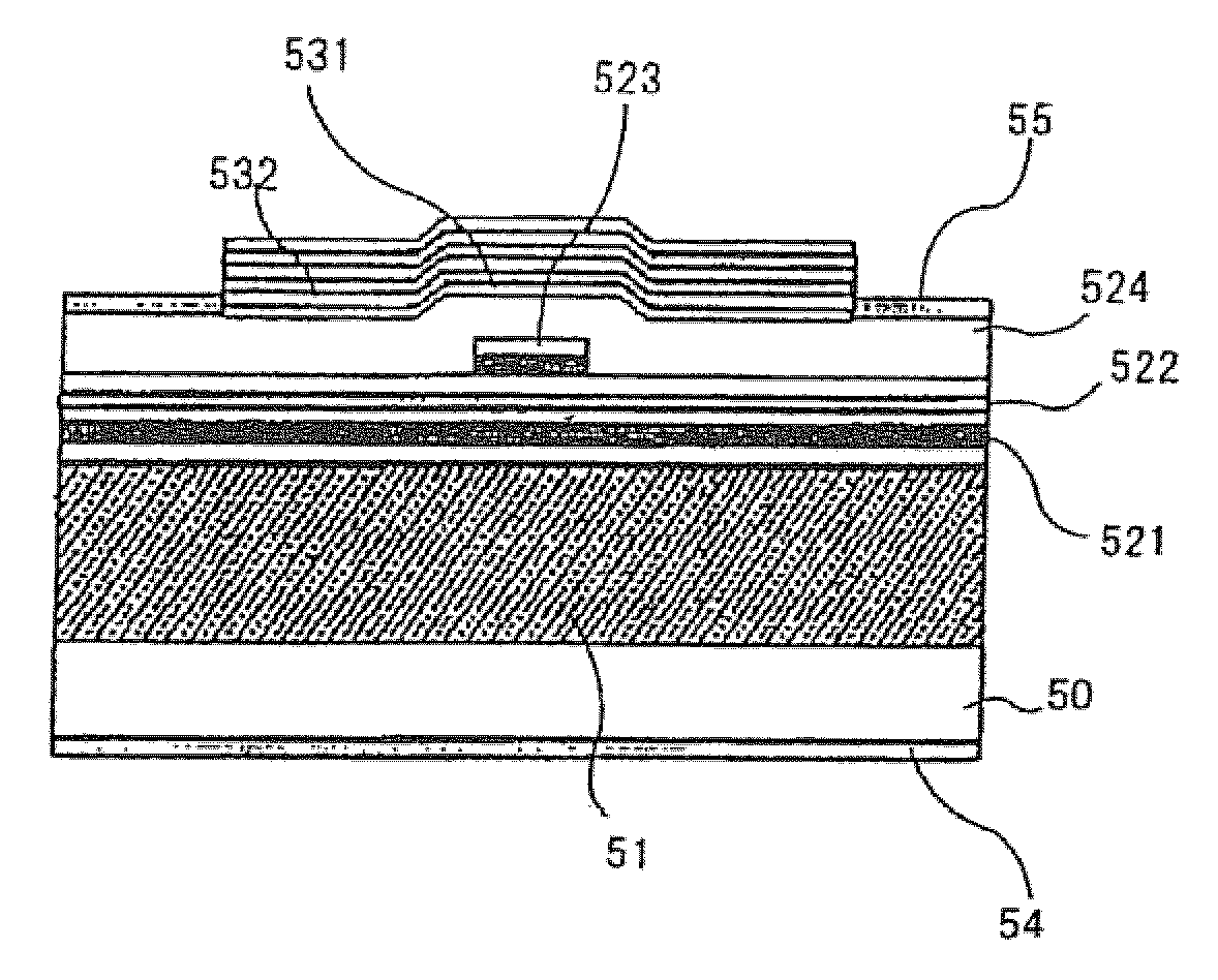
[0122]As shown in FIG. 6A, the surface emitting laser of this Example comprises first multilayer Bragg reflecting mirror 51, second multilayer Bragg reflecting mirror 53, and optical resonator unit 52 sandwiched by these DBRs. First multilayer Bragg reflecting mirror 51 corresponds to an n-type DBR layer, and second multilayer Bragg reflecting mirror 53 corresponds to a dielectric DBR.

[0123]N-type DBR layer 51 includes a plurality of pairs, each of which constitutes a basic unit and is a combination of Si doped GaAs layer 511 which is ...

example 3

[0140]While the current confinement is achieved by tunnel junction 523 in Example 2, an oxide current confinement structure is disposed in part of an n-type semiconductor DBR in this Example.

[0141]FIG. 7 is a schematic diagram showing a band structure of a surface emitting laser according to this Example. While FIG. 7 does not show the vertical axis or horizontal axis, the vertical axis and horizontal axis are similar to those in FIG. 2.

[0142]As shown in FIG. 7, the surface emitting laser of this Example comprises first multilayer Bragg reflecting mirror 61, second multilayer Bragg reflecting mirror 63, and optical resonator unit 62 sandwiched between these DBRs. First multilayer Bragg reflecting mirror 61 corresponds to a lower n-type DBR layer, while second multilayer Bragg reflecting mirror 63 corresponds to an upper dielectric DBR layer.

[0143]Lower n-type DBR layer 61 includes a plurality of pairs, each of which constitutes a basic unit and is a combination of GaAs layer 611 whi...


PUM


Abstract

A surface emitting laser is provided with a first multilayer Bragg reflecting mirror including a first layer, a second multilayer Bragg reflecting mirror including a second layer, and an optical resonator unit that is held between these multilayer Bragg reflecting mirrors and includes an active layer. Further, the optical resonator unit contacts with the first layer and second layer respectively. The effective refraction index neff of the resonator unit is larger than either the first layer or the second layer, and an optical length neffL of the optical resonator unit has a relationship with an oscillating wavelength λ of the surface emitting laser to satisfy the following relationship: 0.5λ<neffL≦0.7λ.

Description

[0001]This application is the National Phase of PCT / JP2007 / 074275, filed Dec. 18, 2007, which is based upon and claims the benefit of priority from Japanese Patent Application No. 2006-352535 filed on Dec. 27, 2006, the content of which is incorporated by reference.TECHNICAL FIELD[0002]The present invention relates to a surface emitting laser which is used in light sources and the like for data communications.BACKGROUND ART[0003]A vertical cavity surface emitting laser (VCSEL) has been widely used as a light source for data communications such as Ethernet (registered trademark) and Fibre Channel due to its low cost and low power consumption properties. These VCSELs have been required to provide such modulation speeds as to support high speed modulation operations at around 10 Gbps (Giga bits per second) in response to an increase in data communication capacity in recent years. Also, the VCSEL is expected as a light source for optical interconnection as well, and devices are increasi...

Claims


Application Information

Patent Timeline
Patent Type & Authority Applications(United States)
IPC IPC(8): H01S5/183
CPCH01S5/06226H01S5/18308H01S5/3095H01S5/18369H01S5/18358
Inventor ANAN, TAKAYOSHISUZUKI, NAOFUMIYASHIKI, KENICHIROTSUJI, MASAYOSHIHATAKEYAMA, HIROSHIFUKATSU, KIMIYOSHIAKAGAWA, TAKESHI
Owner NEC CORP
Why Eureka
Try Eureka