Dry etch stop process for eliminating electrical shorting in MRAM device structures

a technology of mram device structure and dry etch stop, which is applied in the direction of drug composition, metabolic disorder, drug composition, etc., can solve the problems of low selectivity of ion beam milling, easy damage to parts of the stack that are near the edges of the mask or the boundary of an mram cell body, and the profile of mram structure is susceptible to electrical shorting, so as to achieve superior electrical isolation

Active Publication Date: 2010-01-28
OEM GRP LLC
View PDF3 Cites 178 Cited by
  • Summary
  • Abstract
  • Description
  • Claims
  • Application Information

AI Technical Summary

Benefits of technology

[0008]Embodiments of the present invention are directed to, among other things, fabrication of magnetic tunnel junction (MTJ) devices whereby the tunnel barrier layer s...

Problems solved by technology

Ion beam milling operates with low selectivity, and the portions of the stack that are near to the edges of the mask or the boundaries of an MRAM cell body can be easily damaged.
One of the drawbacks of current etching techniques is that the profiles of MRAM structures...

Method used


Image

  • Dry etch stop process for eliminating electrical shorting in MRAM device structures
  • Dry etch stop process for eliminating electrical shorting in MRAM device structures
  • Dry etch stop process for eliminating electrical shorting in MRAM device structures

Examples


Embodiment Construction

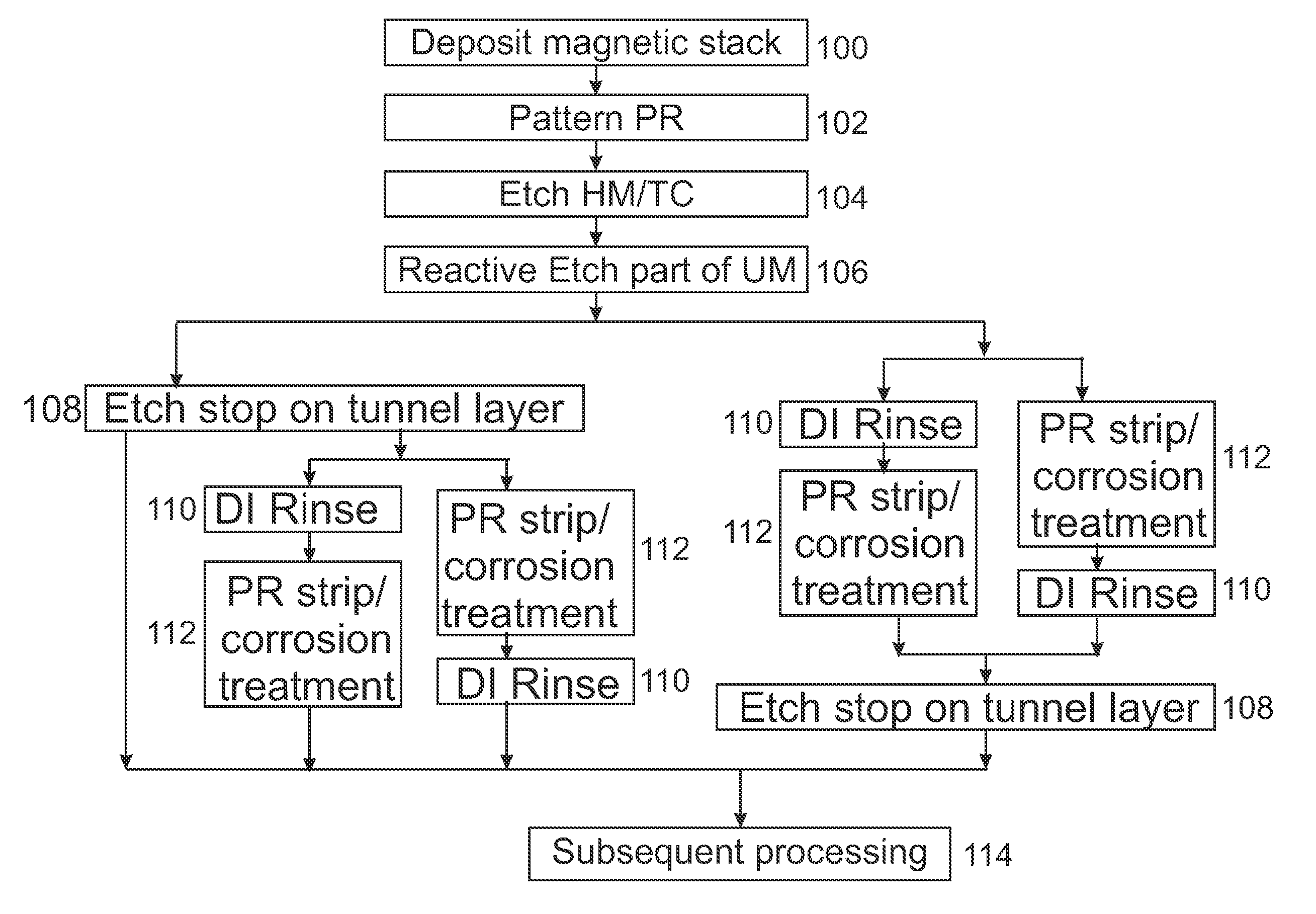
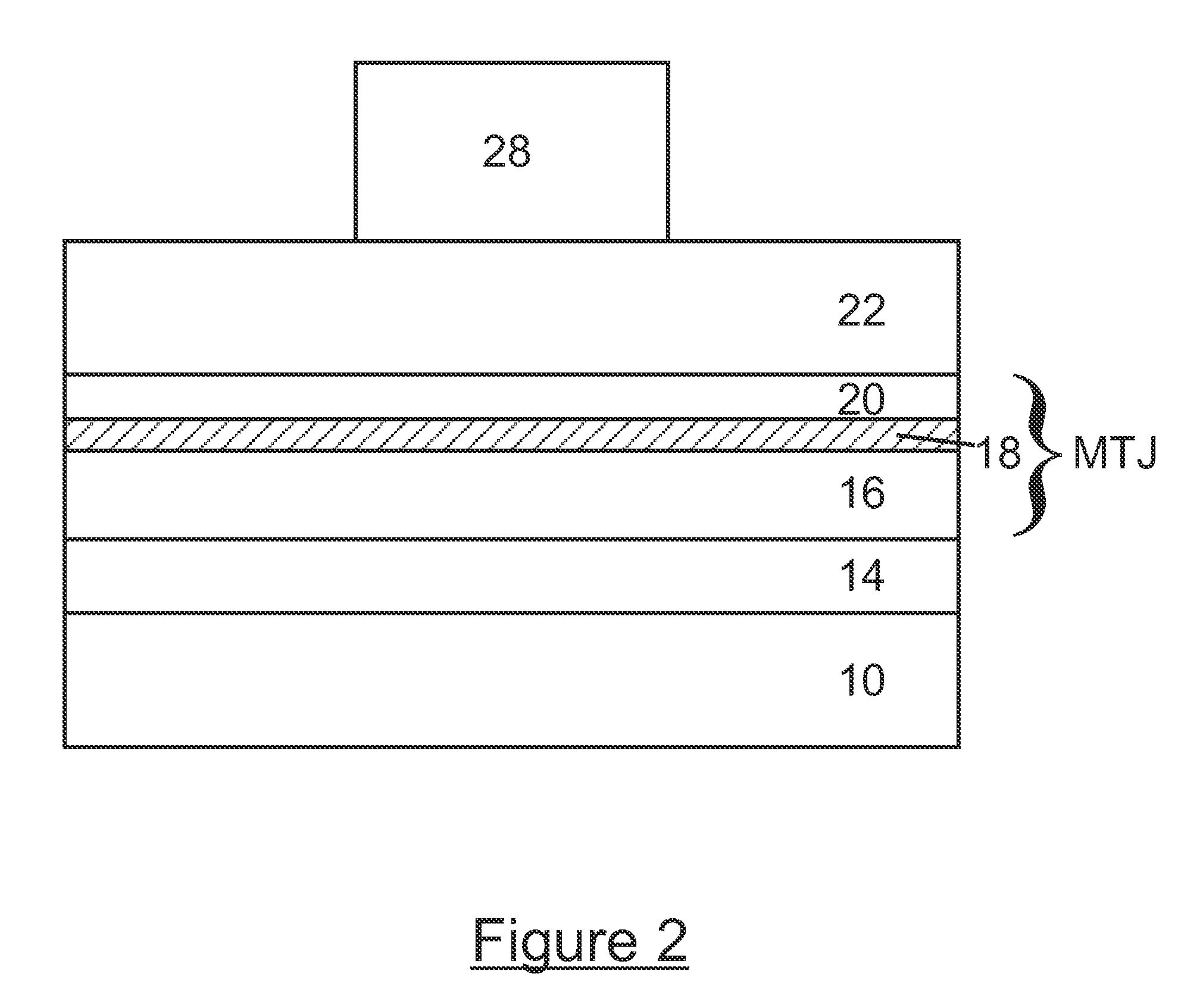
[0028]The present invention is based, in part, on the development of a patterning method for fabricating magnetic tunnel junction (MTJ) devices that are employed in magnetic random access memory (MRAM) devices. As further described herein, a critical aspect of the invention is that MTJ devices prepared by the inventive process afford superior electrical isolation between the magnet layers in contact with the dielectric tunnel layer in comparison to the current art.

[0029]A typical MRAM structure, within which an MTJ is contained, is shown in FIG. 1. The MRAM structure is a complex stack of magnetic, conductive, and insulating films on a substrate. In FIG. 1, the specific components of a typical MRAM structure are shown and consist of a substrate 10, a barrier layer 12, a bottom contact layer 14, a multilayer fixed magnet structure 16 consisting of layers of CoFe, Ru, NiFe, IrMn, PtMn, and the like, a dielectric tunnel layer such as alumina or MgO 18, a switchable magnet layer 20 (NiF...


PUM

PropertyMeasurementUnit
Fractionaaaaaaaaaa
Fractionaaaaaaaaaa
Fractionaaaaaaaaaa

Abstract

The present invention relates generally to semiconductor fabrication and particularly to fabricating magnetic tunnel junction devices. In particular, this invention relates to a method for using the dielectric layer in tunnel junctions as an etch stop layer to eliminate electrical shorting that can result from the patterning process.

Description

CLAIM TO PRIORITY[0001]This application claims priority to all of the following applications including U.S. patent application Ser. No. 11 / 724,556, filed Mar. 14, 2007 entitled “DRY ETCH STOP PROCESS FOR ELIMINATING ELECTRICAL SHORTING IN MRAM DEVICE STRUCTURES” (Attorney Docket No. TEGL-01247US1); and[0002]U.S. Provisional Application No. 60 / 783,157, filed Mar. 16, 2006 entitled “DRY ETCH STOP PROCESS FOR ELIMINATING ELECTRICAL SHORTING IN MRAM DEVICE STRUCTURES” (Attorney Docket No. TEGL-01247US0).FIELD OF THE INVENTION[0003]The present invention relates generally to semiconductor fabrication and particularly to fabricating device structures containing metal-insulator-metal layered thin film stacks such as those used in magnetic tunnel junction devices and memory devices.BACKGROUND OF THE INVENTION[0004]Layered films of metal-insulator-metal are employed as storage elements in memory devices such as magnetic random access memories (MRAM) and the like. The memory element for the MR...

Claims


Application Information

Patent Timeline
IPC IPC(8): H01L43/12C23F1/00
CPCC07D401/04A61P3/10A61P9/04A61P9/10A61P17/02A61P25/00A61P25/06A61P27/02A61P29/00A61P35/00A61P43/00A61K31/506C07D401/14
Inventor DITIZIO, ROBERT ANTHONY
Owner OEM GRP LLC
Why Eureka
Try Eureka