Modulated metal removal using localized wet etching

a wet etching and module technology, applied in the direction of electrical equipment, decorative surface effects, decorative arts, etc., can solve the problems of large number of low aspect ratios, uneconomical depositing of thick metal layers, and more rugged and complex topography by adding additional layers

Active Publication Date: 2010-02-04
NOVELLUS SYSTEMS
View PDF79 Cites 73 Cited by
  • Summary
  • Abstract
  • Description
  • Claims
  • Application Information

AI Technical Summary

Benefits of technology

[0015]The invention helps to solve some of the problems and to satisfy some of the needs mentioned above by providing systems, apparatuses, methods and compositions for controlled, localized chemical wet etching of metal from integrated circuit substrates. Control of cumulative etching in one or more local etch regions over a total etching process time is achieved by modulating the flow of etching liquid in at least one area of the substrate surface. A feature of embodiments in accordance with the invention is localized metal etching, compared to more common global treatments of the prior art. Localized wet etching of a semiconductor wafer is better able than global techniques to address non-uniformities on a macroscopic scale, for example, differences in metal thicknesses between different areas across a substrate wafer. Embodiments in accordance with the invention help to solve the problem of highly variable and difficult-to-control topography that commonly results from damascene copper electroplating processes.
[0020]In some embodiments, the wafer holder, the semiconductor wafer, the etch nozzles and the rinse nozzle are located in a treatment container, and the method further comprises positioning a retractable splash shield in an active position (e.g., in a vertical up position around the wafer periphery, or in a horizontal closed position above the wafer) while applying the etching liquid to the semiconductor. In some embodiments, a vertical splash shield substantially surrounds the semiconductor wafer in the wafer holder and is located between the wafer holder and an outer wall of the treatment container to inhibit etching liquid from splashing onto the outer wall. During rinsing, the inner vertical movable splash shield is in a down (or inactive) position so that the vertical rinse shield is not proximate to the surface plane of the semiconductor wafer in the wafer holder.
[0025]A basic embodiment of an apparatus for removing metal from a semiconductor wafer using localized wet etching comprises: a wafer holder for supporting and rotating a semiconductor wafer; and a plurality of etch nozzles. Use of a plurality of etch nozzles has a number of advantages, including, but not limited to: 1) allowing the control of the etching rate profile over the wafer; 2) applying different flow rates to different regions of the wafer; 3) applying different chemicals or chemical concentrations at various times during the process to different impact zones of the wafer; and 4) minimizing the total required amount of etchant (etching liquid) supplied to the wafer surface to achieve uniform etching (e.g., relative to a single nozzle that would spray the entire wafer simultaneously). A first etch nozzle is operable for applying a first flow pattern of etching liquid to form a first band-like impact zone of etching liquid on a rotating semiconductor wafer. A second etch nozzle is operable for applying simultaneously a second flow pattern of etching liquid to form a second, band-like impact zone of the etching liquid on the rotating semiconductor wafer that is spatially distinct from other impact zones. The first etch nozzle is operable for modulating the first flow pattern of etching liquid to selectively control a first cumulative etching rate in a first local etch region of the semiconductor wafer relative to a second cumulative etching rate in a second local etch region. Preferably but not necessarily, each of the first etch nozzle and the second etch nozzle is operable to apply a 3-dimensional flow pattern of etching liquid that extends beyond peripheral edges of a semiconductor wafer. In some embodiments, the first etch nozzle is operable for modulating the first flow pattern of etching liquid using one or a combination of the following techniques: by ceasing flow of etching liquid; by ceasing flow of etching liquid and then applying deionized water to the first impact zone; by ceasing flow of etching liquid and then applying an etching quenchant to the first impact zone; by changing a flow rate of etching liquid; by changing a composition of etching liquid; by changing a concentration of etching liquid; by changing the location of the impact zone, and, by changing a shape of the first flow pattern. In some embodiments, the first etch nozzle and the second etch nozzle are operable to apply etching liquid substantially normal to the surface of a semiconductor wafer, thereby maximizing the amount of convective mixing and defining a relatively small region of high impacting fluid.
[0029]Some embodiments of an apparatus further comprise: a treatment container in which the wafer holder and the etch nozzles are located; and a retractable vertical splash shield that is operable in an up (shielding, or active) position and in a down (or non-shielding inactive) position. The vertical splash shield in the up position substantially surrounds a semiconductor wafer in the wafer holder and is located between the wafer holder and an inner wall of the treatment container and serves to inhibit etching liquid from etch nozzles and from a spinning semiconductor wafer from splashing onto the inner wall. The vertical splash shield may consist of a reticulated bellows-like conical element, which can collapse to a relatively small vertical dimension when retracted. In some embodiments, the treatment container includes a nozzle-arm alcove to which the nozzle arm is movable so that the nozzle arm and the plurality of etch nozzles are not directly above the wafer holder. Some embodiments further comprise a rinse nozzle for rinsing a semiconductor wafer.

Problems solved by technology

As the number of levels in an interconnect technology is increased, the stacking of additional layers produces more rugged and complex topography.
Baths with good “bottom-up” filling characteristics fill high aspect ratio features more rapidly and without creating void or seam when compared to baths with less effective combinations of such additives.
The use of advanced “bottom-up” electrofilling techniques with wafers having both low and high aspect-ratio features has created a problem of deposited metal surfaces with a wide range of topography, that is, topography containing a large range of height and width variations in both recessed and raised areas.
Therefore, while electroplating is the preferred method of metallization, various aspects of improved plating regimens create challenging topography for subsequent planarization.
These approaches and techniques generally require overburden.
A problem sometimes arises during processing of surfaces in which a large number of low aspect-ratio (larger width than depth) features exist.
Depositing a thick metal layer would be uneconomical due to necessary removal of the large excess of metal at a later stage.
This is an unacceptable result.
Traditionally, stacked ICs are interconnected together along their edges using wires, but such wiring can have a limited bandwidth, and increases the stack's dimensions and usually requires extra layers between the ICs.
Similar problems may arise from chemical (nonelectrolytic) wet etching of metal from a substrate surface.
In some circumstances, if chemical wet etching were conducted long enough to remove substantially the metal over field areas and above “overplated” high-aspect-ratio features of a nonplanar substrate, then excessive over-etching of metal and generation of recesses in low-aspect-ratio features would result.

Method used


Image

  • Modulated metal removal using localized wet etching
  • Modulated metal removal using localized wet etching
  • Modulated metal removal using localized wet etching

Examples


example 1

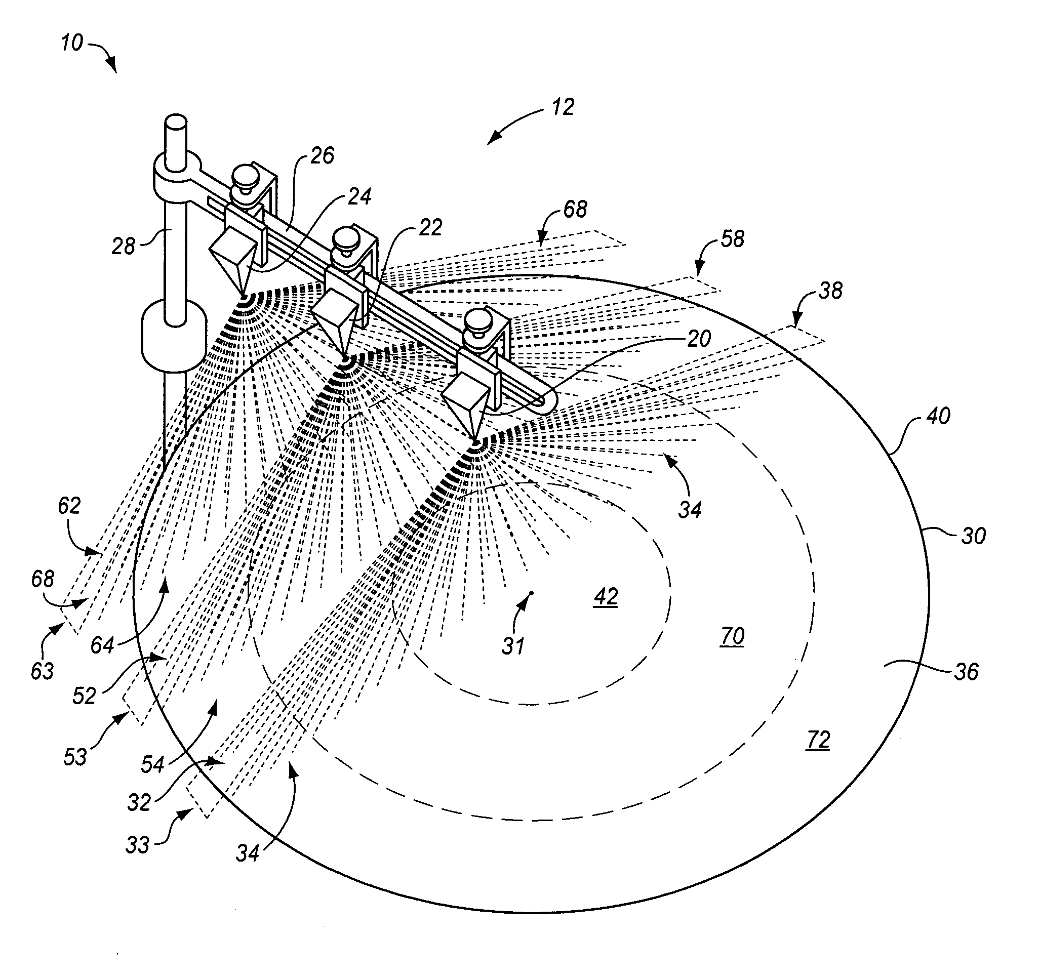
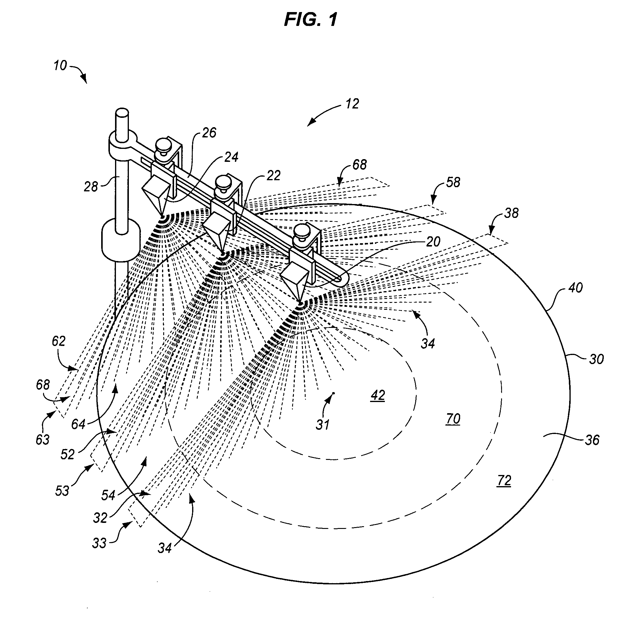
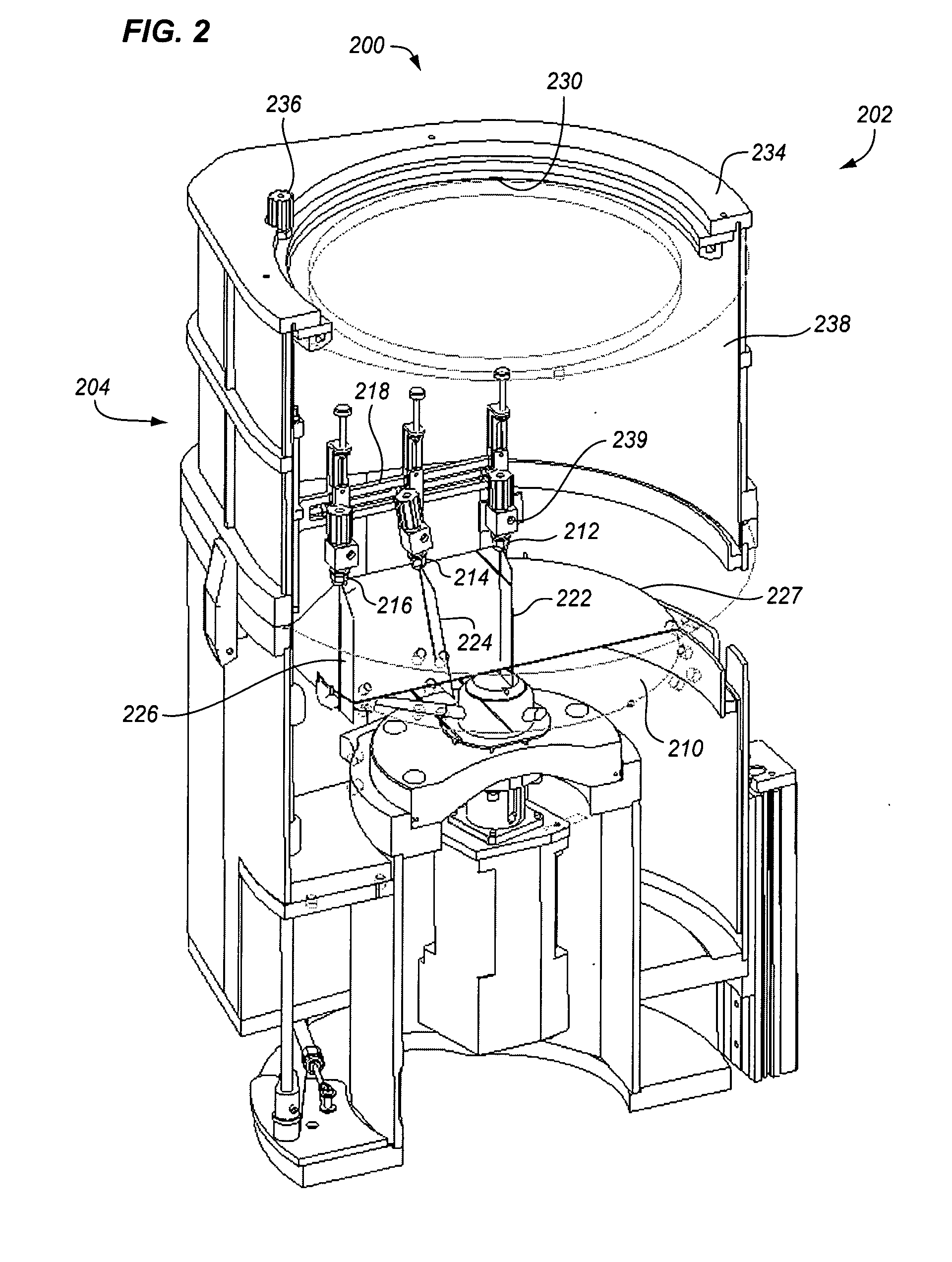
[0091]Copper was removed from 300 mm semiconductor wafers using localized wet etching in accordance with the invention. Using conventional techniques, a seed layer was formed on each wafer, then a layer of copper was electroplated onto the seed layer. The wafer was etched without delay and with high-temperature thermal annealing. The etching solution after all components were combined and mixed consisted essentially of: H2O2 at 1.06 molar concentration and glycine at 0.066 molar concentration in deionized water having a pH value of 8.9. The etching rate typically associated with the etching solution is about 1000 Å per minute. Etching liquid was applied to the semiconductor wafers using an apparatus in accordance with the invention having a center nozzle and an edge nozzle. During etching operations, flow of etching solution liquid through a particular nozzle was either on or off. When flow through the center nozzle was switched on, the etching liquid flow rate through that nozzle w...


PUM

PropertyMeasurementUnit
radial widthaaaaaaaaaa
radial distanceaaaaaaaaaa
feature widthsaaaaaaaaaa

Abstract

An apparatus for wet etching metal from a semiconductor wafer comprises a wafer holder for rotating a wafer and a plurality of nozzles for applying separate flow patterns of etching liquid to the surface of the wafer. The flow patterns impact the wafer in distinct band-like impact zones. The flow pattern of etching liquid from at least one nozzle is modulated during a total etching time control the cumulative etching rate in one local etch region relative to the cumulative etching rate in one or more other local etch regions. Some embodiments include a lower etch chamber and an upper rinse chamber separated by a horizontal splash shield. Some embodiments include a retractable vertical splash shield used to prevent splashing of etching liquid onto the inside walls of a treatment container. An etch-liquid delivery system includes a plurality of nozzle flow paths having corresponding nozzle flow resistances, and a plurality of drain flow paths having corresponding drain flow resistances. Nozzle flow resistances and drain flow resistances are matched so that switching the flow from a nozzle to a corresponding drain flow path does not change the flow rate of etching liquid through other nozzles. A non-wafer-contacting measuring device measures a metal thickness on a rotating semiconductor wafer during metal wet etching by immersing a plurality of electrodes in etching liquid in close proximity to the wafer surface of the rotating wafer and determining electrical resistance between a plurality of electrodes.

Description

RELATED APPLICATIONS[0001]This application is a continuation-in-part application, claiming priority under 35 USC 120, of co-owned and co-pending U.S. patent application Ser. No. 11 / 602,128, filed Nov. 20, 2006, by Mayer et al., having the title “Topography Reduction and Control by Selective Accelerator Removal”, which claims the benefit under 35 USC 119(e) of U.S. Provisional Application Ser. No. 60 / 737,978, filed Nov. 19, 2005, by Mayer et al. This application is also a continuation-in-part application, claiming priority under 35 USC 120, of co-owned and co-pending U.S. patent application Ser. No. 11 / 888,312, filed Jul. 30, 2007, by Koos et al., titled “Fabrication of Semiconductor Interconnect Structure”, which is a continuation-in-part application of U.S. patent application Ser. No. 11 / 586,394, filed Oct. 24, 2006, by Koos et al., now U.S. Pat. No. 7,531,463, which was a continuation-in-part application of U.S. patent application Ser. No. 10 / 690,084, filed Oct. 20, 2003, by Koos ...

Claims


Application Information

Patent Timeline
Patent Type & Authority Applications(United States)
IPC IPC(8): H01L21/306
CPCC23F1/08C23F1/34H01L21/6708H01L21/32115H01L21/32134C25F3/12
Inventor MAYER, STEVEN T.PORTER, DAVID W.
Owner NOVELLUS SYSTEMS
Why Eureka
Try Eureka