Bi-directional DMOS with common drain

Active Publication Date: 2010-02-11
TEXAS INSTR INC
View PDF9 Cites 21 Cited by
  • Summary
  • Abstract
  • Description
  • Claims
  • Application Information

AI Technical Summary

Problems solved by technology

Bi-directional configurations of high voltage transistors, in which source and drain roles may be reversed, exhibit increase

Method used


Image

  • Bi-directional DMOS with common drain
  • Bi-directional DMOS with common drain
  • Bi-directional DMOS with common drain

Examples


first embodiment

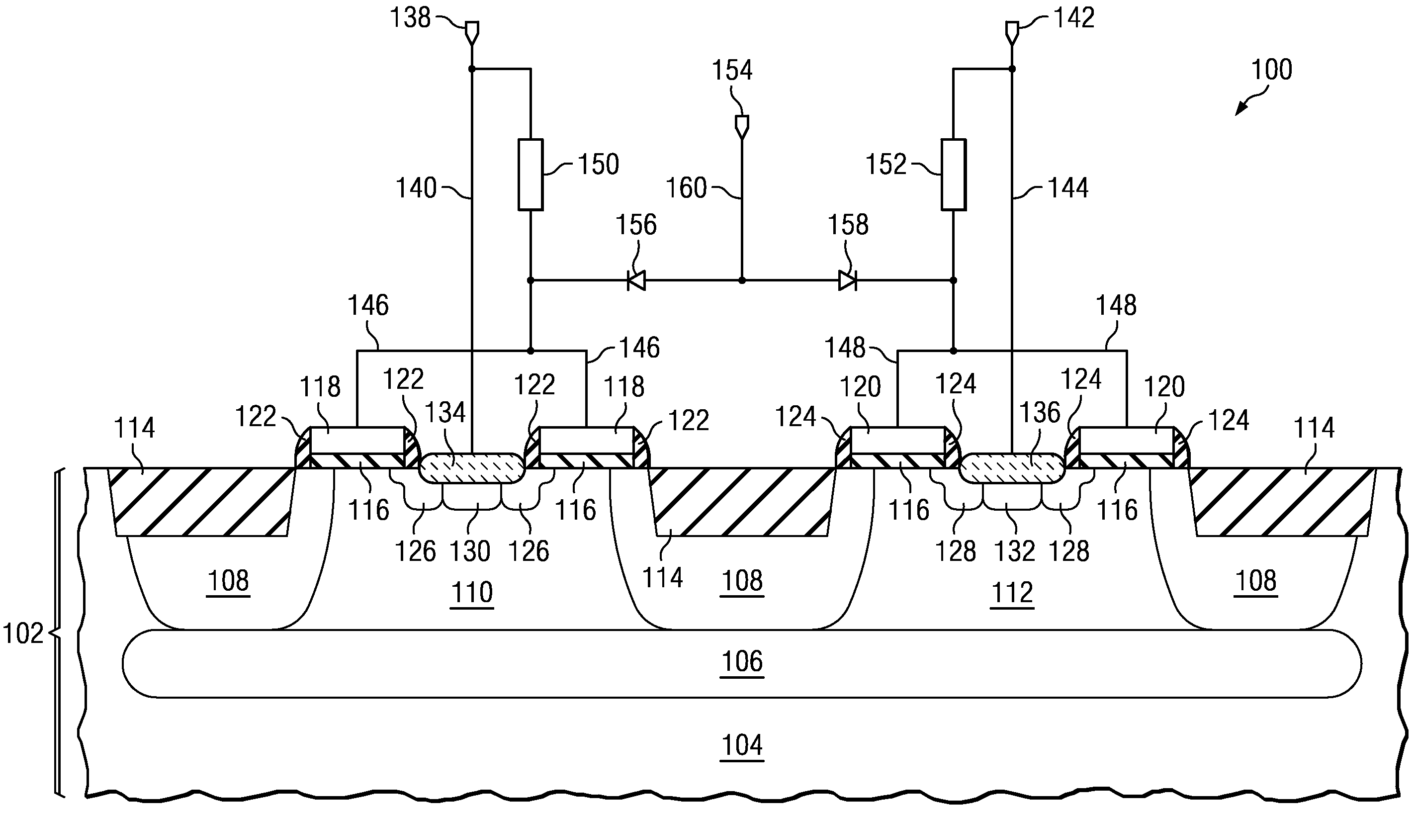
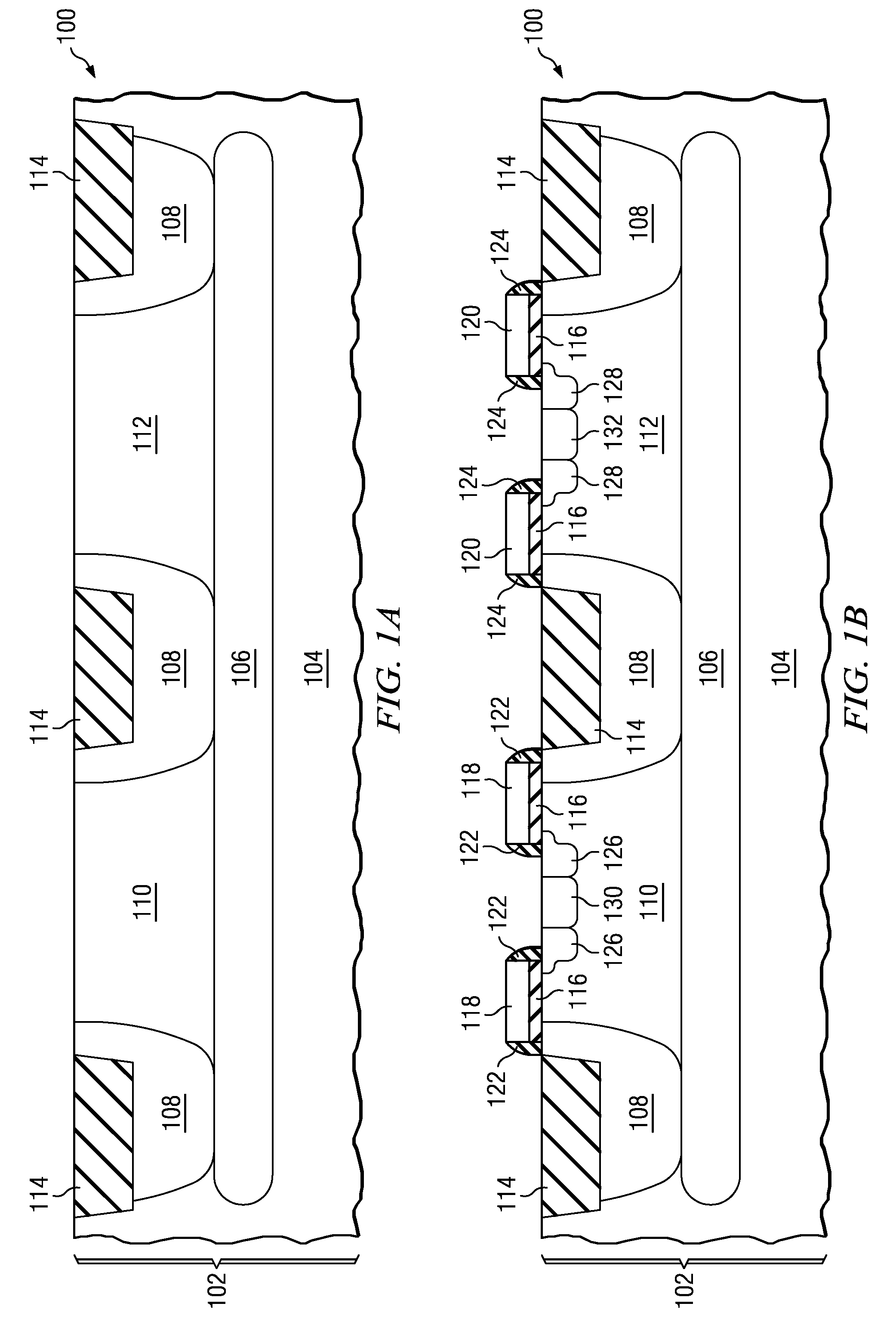
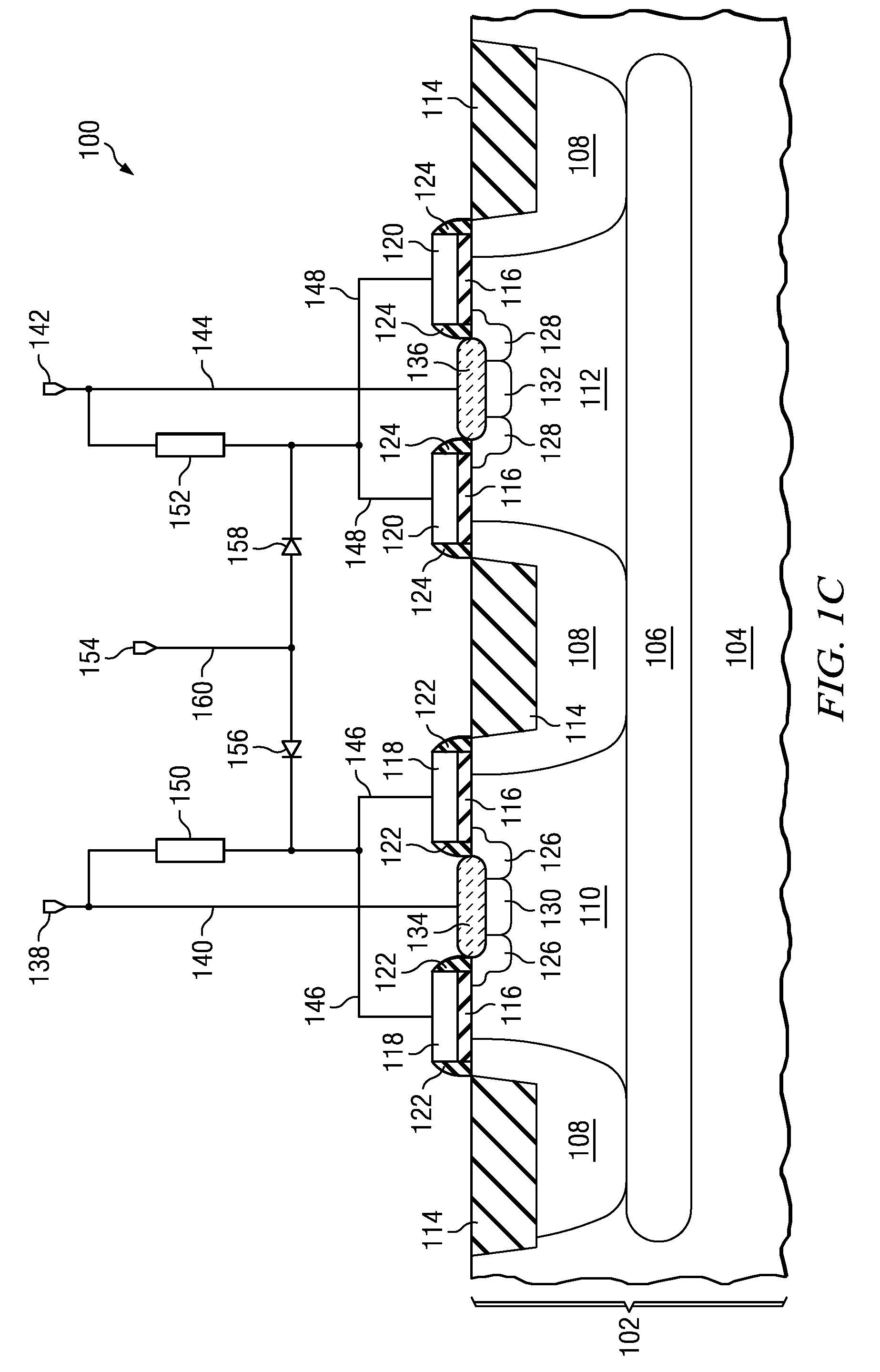
[0015]FIG. 1A through FIG. 1C are cross-sections of the instant invention depicted in successive stages of fabrication. Referring to FIG. 1A, an IC 100 is formed in a substrate 102, typically p-type single crystal silicon, but possibly a silicon-on-insulator (SOI) wafer, a hybrid orientation technology (HOT) wafer, or any other substrate appropriate for supporting the fabrication of the IC 100. Substrate material 104 near a top surface of the substrate 102 is p-type. An n-type buried layer (NBL) 106 is formed in the substrate in an area defined for the bi-directional LDMOS transistor using known methods, typically including ion implanting an NBL set of n-type dopants, commonly antimony, and possibly arsenic and / or phosphorus, at a total dose between 1·1015 and 1·1016 cm−2, into a top region of the substrate 102 followed by epitaxial growth of 2 to 5 microns of p-type semiconductor material on a top surface of the substrate 102 and NBL 106.

[0016]Still referring to FIG. 1A, a deep n-w...

second embodiment

[0035]FIG. 2A through FIG. 2C are cross-sections of the instant invention depicted in successive stages of fabrication. Referring to FIG. 2A, an IC 200 is formed in a substrate 202 with the properties described in reference to FIG. 1A. Substrate material 204 near a top surface of the substrate 202 is p-type. A deep n-well 206 is formed in the substrate 202, by processes described in reference to FIG. 1A, extending from the top surface of the substrate 202 to a depth between 2 and 5 microns. Optional elements of field oxide 208 are formed by STI processes, as described in reference to FIG. 1A, to isolate elements of the three terminal bi-directional LDMOS.

[0036]Still referring to FIG. 2A, a first p-type backgate well 210 and a second p-type backgate well 212 are formed in the deep n-well 206, using known methods, for example ion implanting a p-well set of p-type dopants, typically boron, at a total dose between 1·1013 and 3·1014 cm−2, into areas of the deep n-well 206 defined for the...

third embodiment

[0044]FIG. 3A through FIG. 3C are cross-sections of the instant invention depicted in successive stages of fabrication. Referring to FIG. 3A, an IC 300 is formed in a substrate 302 with the properties described in reference to FIG. 1A. Substrate material 304 near a top surface of the substrate 302 is p-type. An NBL 306 is formed in the substrate in an area defined for the bi-directional LDMOS transistor using known methods, as described in reference to FIG. 1A, followed by epitaxial growth of 2 to 5 microns of p-type semiconductor material on a top surface of the substrate 302 and NBL 306. A deep n-well 308 is formed in the substrate 302 in a drain area of the three terminal bi-directional LDMOS, by processes described in reference to FIG. 1A, extending from the top surface of the substrate 302 to the NBL 306. Deep n-type diffused regions known a n-sinkers 310 are formed in the substrate 302 around the area defined for the bi-directional LDMOS transistor, extending from the top surf...


PUM


Abstract

A three terminal bi-directional laterally diffused metal oxide semiconductor (LDMOS) transistor which includes two uni-directional LDMOS transistors in series sharing a common drain node, and configured such that source nodes of the uni-directional LDMOS transistors serve as source and drain terminals of the bi-directional LDMOS transistor. The source is shorted to the backgate of each LDMOS transistor. The gate node of each LDMOS transistor is clamped to its respective source node to prevent source-gate breakdown, and the gate terminal of the bi-directional LDMOS transistor is connected to the gate nodes of the constituent uni-directional LDMOS transistors through blocking diodes. The common drain is a deep n-well which isolates the two p-type backgate regions. The gate node clamp can be a pair of back-to-back zener diodes, or a pair of self biased MOS transistors connected source-to-source in series.

Description

FIELD OF THE INVENTION[0001]This invention relates to the field of integrated circuits. More particularly, this invention relates to high voltage transistors in integrated circuits.BACKGROUND OF THE INVENTION[0002]Lateral diffused metal oxide semiconductor (LDMOS) transistors and drain extended metal oxide semiconductor (DEMOS) transistors in integrated circuits (ICs) provide a desirable capability of modulating voltages which exceed breakdown limits of gate dielectrics in the LDMOS and DEMOS transistors. LDMOS and DEMOS transistors are uni-directional devices, in which voltages exceeding the breakdown limits of the gate dielectrics must be applied to the drain nodes, but not the source nodes. Bi-directional configurations of high voltage transistors, in which source and drain roles may be reversed, exhibit increased series resistance or require thick gate dielectric layers which are problematic to integrate into IC fabrication processes.SUMMARY OF THE INVENTION[0003]This Summary is...

Claims


Application Information

Patent Timeline
IPC IPC(8): H01L27/06H01L21/8234
CPCH01L21/823425
Inventor PENDHARKAR, SAMEER P.
Owner TEXAS INSTR INC
Why Eureka
Try Eureka