Semiconductor element, method for manufacturing same, and electronic device including same

a semiconductor element and method technology, applied in the direction of semiconductor devices, basic electric elements, electrical appliances, etc., can solve the problems of not being able to suppress the deterioration of transistor characteristics, not being able to obtain a crystallized thin zinc oxide film unlike silicon, and being difficult to achieve a crystallized thin zinc oxide film. , to achieve the effect of improving the tft characteristic of the semiconductor element, reducing the influence of grain boundary, and enhancing the performance of an electronic devi

Active Publication Date: 2010-02-25
SHARP KK +1
View PDF15 Cites 37 Cited by
  • Summary
  • Abstract
  • Description
  • Claims
  • Application Information

AI Technical Summary

Benefits of technology

[0049]In an active matrix display device such as a liquid crystal display device and an organic EL display device, a switching element is turned on when an image signal is written from a driving circuit into a pixel electrode. Further, in an image reading apparatus such as an image sensor, a switching element is turned on when a pixel signal in a pixel electrode is read out. That is, according to the above arrangement, it is possible to realize (i) an active matrix display device including a semiconductor element of the present invention as a switching element and (ii) an image reading apparatus including a semiconductor element of the present invention as a switching element. Therefore, it is possible to easily enhance performance of an electronic device such as an active matrix display device and an image reading apparatus.
[0050]As described above, a semiconductor element of the present invention includes as an active layer a polycrystalline ZnO film in which impurities are added more in concentration to a grain boundary part than to a crystal part. This allows an energy level of a trap level formed on a grain boundary of the active layer to be shifted to a level which does not influence an energy level of carriers. This allows a reduction in influence of the grain boundary on operation of a semiconductor element, thus allowing an improvement in TFT characteristic of the semiconductor element such as electron field-effect mobility and subthreshold coefficient S.

Problems solved by technology

However, each of the Patent Literatures 1 through 3 does not address anything about the suppression of influence of a grain boundary on a transistor characteristic.
That is, according to the technique disclosed in the Patent Literatures 1 through 3, it is not possible to suppress a deterioration in transistor characteristic due to a grain boundary, in a case where an active layer is made of a polycrystalline ZnO film.
Further, since zinc oxide has a high melting point of 2000° C., it is difficult to obtain a crystallized thin zinc oxide film unlike silicon.
That is, in a case where a polycrystalline ZnO film is used as an active layer, it is not possible for the SOI technique to suppress a deterioration in transistor characteristic due to a grain boundary.
As described above, the conventional art cannot suppress a deterioration in transistor characteristic due to a grain boundary in a case where a polycrystalline ZnO film is used as an active layer.

Method used


Image

  • Semiconductor element, method for manufacturing same, and electronic device including same
  • Semiconductor element, method for manufacturing same, and electronic device including same
  • Semiconductor element, method for manufacturing same, and electronic device including same

Examples


embodiment 1

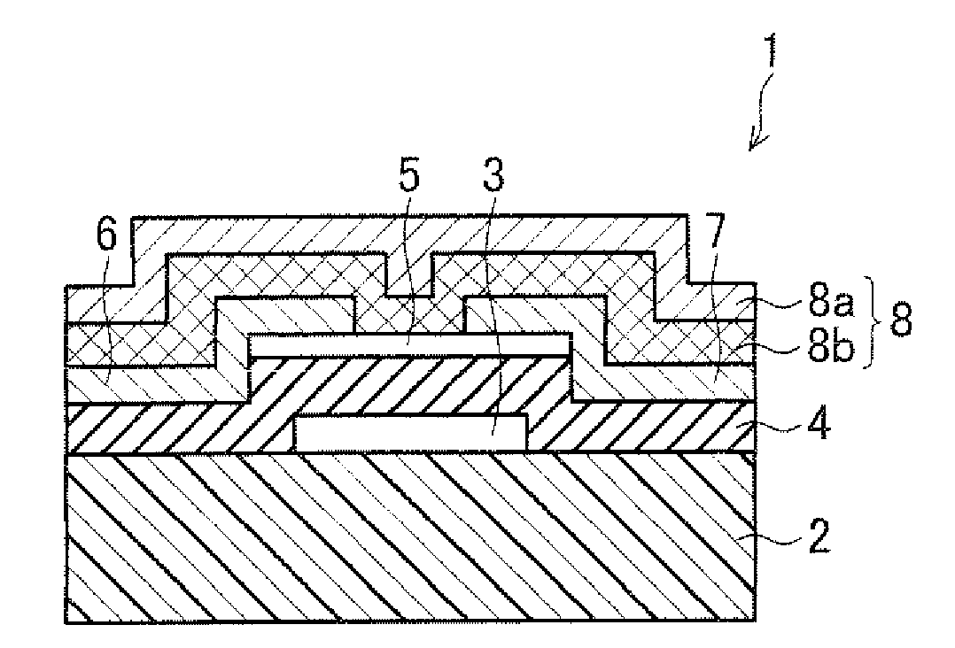
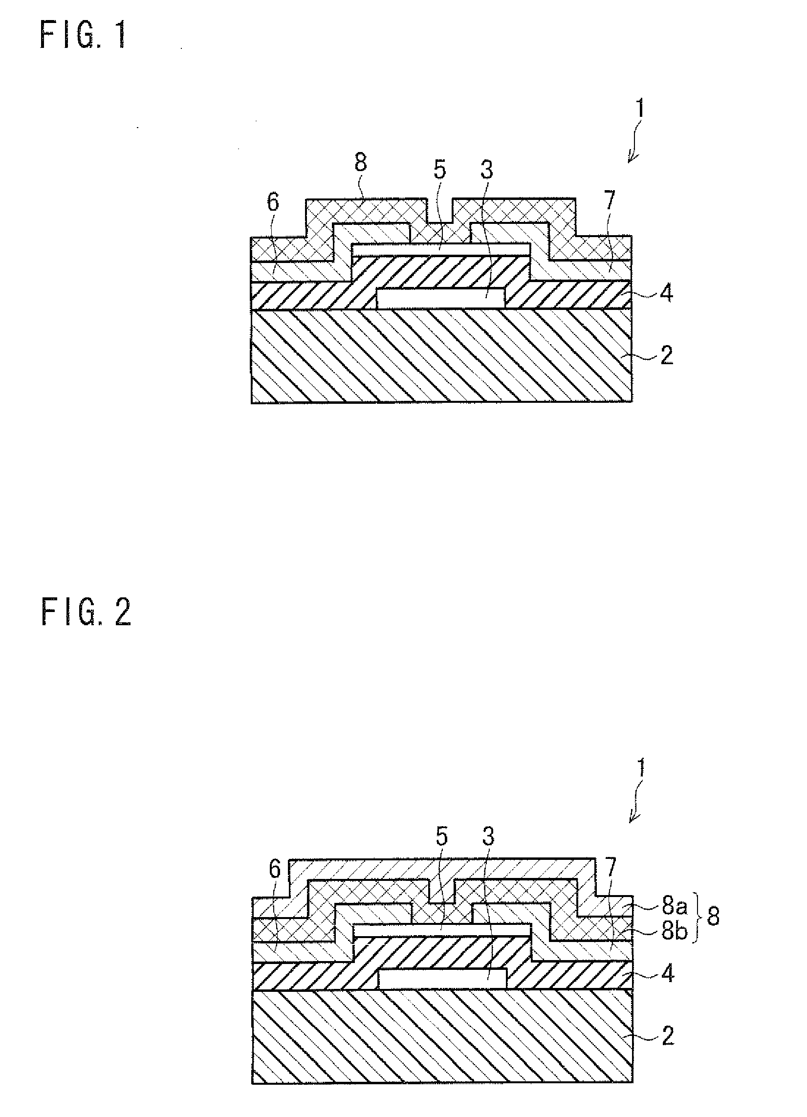
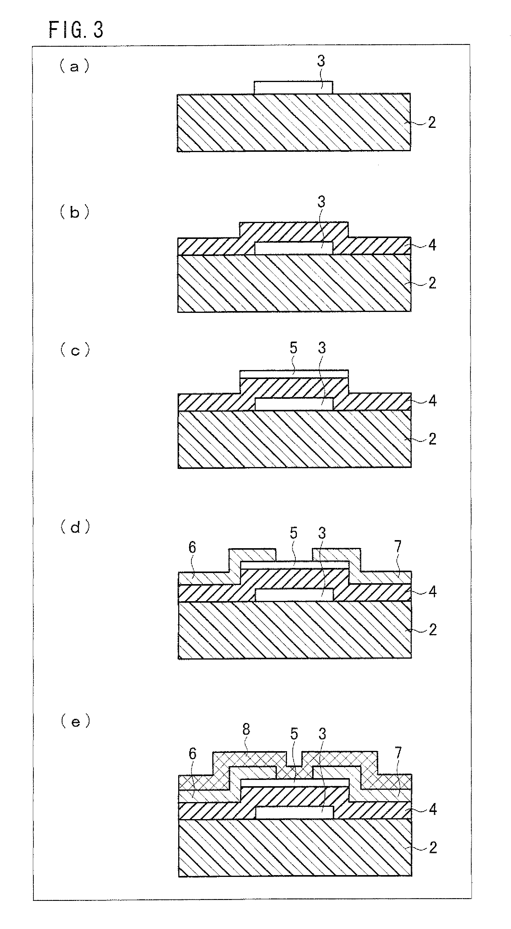
[0065]As shown in FIG. 1, a thin-film transistor 1 of the present embodiment includes an insulating substrate 2, a gate electrode 3, a gate insulating layer 4, a semiconductor layer 5, a source electrode 6, a drain electrode 7, and a protection layer 8. The gate electrode 3 is provided on the insulating substrate 2. The semiconductor layer 5 is provided so as to be stacked above the gate electrode 3 via the gate insulating layer 4. Further, the source electrode 6 and the drain electrode 7 are provided, as respective electrode sections, on the semiconductor layer 5. The source electrode 6 and the drain electrode 7 are connected to each other via the semiconductor layer 5. Furthermore, the protection layer 8 is provided so as to cover the semiconductor layer 5, the source electrode 6, and the drain electrode 7. That is, the thin-film transistor 1 has an inversely staggered structure.

[0066]Further, in a case where the thin-film transistor 1 is used in a display device (e.g. a later des...

embodiment 2

[0106]Another embodiment of the present invention is described below with reference to FIGS. 4 and 5. For convenience of explanation, constituents which have identical functions to those of the Embodiment 1 are given identical reference numerals, and are not explained repeatedly.

[0107]A display device 10 of the present embodiment is an active matrix liquid crystal display device. As shown in FIG. 4, the display device 10 includes a pixel array 31, a source driver 32, a gate driver 33, a control circuit 34, and a power supply circuit 35.

[0108]Each of the pixel array 31, the source driver 32, and the gate driver 33 is formed on a substrate 36. The substrate 36 is made of a material having insulation properties and light-transmitting properties (e.g. glass). The pixel array 31 includes source lines SL, gate lines GL, and pixels 37.

[0109]In the pixel array 31, a plurality of gate lines GLj, GLj+1 . . . intersect with a plurality of source lines SLi, SLi+1 . . . , and a pixel 37 (PIX in ...

example 1

Study of Conditions Under which Impurities are Added to an Active Layer

[0145]A semiconductor element of the present invention includes an active layer in which impurities are added to polycrystalline ZnO film. That is, in manufacturing the semiconductor element of the present invention, it is necessary to add the impurities to the polycrystalline ZnO film. It is necessary that the impurities are added to the polycrystalline ZnO film under a condition such that ZnO of the polycrystalline ZnO film to which the impurities are added does not dissolve. In view of this, this example studied an adding condition under which sulfur was added to a polycrystalline ZnO film with the use of the CBD method so that ZnS was formed in a grain boundary. Used as a solution in the CBD method is a solution for forming ZnS (zinc sulfide) film which contains ZnSO4.7H2O (Zn precursor), SC(NH2)2 (sulfur precursor), and an ammonia solution (complexing agent).

[0146]FIG. 6 shows a relationship between concentr...


PUM


Abstract

A thin-film transistor (1) of the present invention includes an insulating substrate (2), a gate electrode (3) which has a predetermined shape and is formed on the insulating substrate (2), a gate insulating film (4) formed on the gate electrode (3), and a semiconductor layer (5) which is polycrystalline ZnO and is formed on the gate insulating film (4). The semiconductor layer (5) is immersed in a solution in which impurities are dissolved so that the impurities are selectively added to a grain boundary part of the polycrystalline ZnO film. Subsequently, a source electrode (6) and a drain electrode (7) are formed so as to have a predetermined shape. Next, a protection layer (8) is formed on the source electrode (6) and the drain electrode (7). Thus, a thin-film transistor which has a good subthreshold characteristic and has a zinc oxide film as a base of an active layer can be realized.

Description

TECHNICAL FIELD[0001]The present invention relates to (i) a semiconductor element, (ii) a method for manufacturing the semiconductor element, and (iii) an electronic device including the semiconductor element. The present invention especially relates to (i) a semiconductor element which has a zinc oxide film serving as a base of an active layer, (ii) a method for manufacturing the semiconductor element, and (iii) an electronic device including the semiconductor element.BACKGROUND ART[0002]In recent years, there has been rapidly expanded in use of a flat panel display (FPD) device such as a liquid crystal display device or an organic EL (electroluminescence) display device. Among them, an active matrix display device is exemplified as a flat panel display device which can carry out a high grade display.[0003]The active matrix display device adopts amorphous silicon TFTs (Thin-Film Transistors) or polysilicon TFTs (Thin-Film Transistors). Such amorphous silicon TFTs (Thin-Film Transis...

Claims


Application Information

Patent Timeline
Patent Type & Authority Applications(United States)
IPC IPC(8): H01L29/12H01L21/20
CPCH01L29/78696H01L29/7869Y10S438/922
Inventor URAYAMA, MASAOKAWASAKI, MASASHIOHNO, HIDEO
Owner SHARP KK
Why Eureka
Try Eureka