Apparatus and method for edge bevel removal of copper from silicon wafers

a technology of edge bevel removal and silicon wafers, which is applied in the direction of electrostatic cleaning, cleaning processes and apparatus, chemical apparatus and processes, etc., can solve the problems of significant process impediments and compromise of edge bevel etching process quality, etc., to promote diffusion, enhance etching rate, and high speed rotation

Active Publication Date: 2010-03-04
NOVELLUS SYSTEMS
View PDF60 Cites 44 Cited by
  • Summary
  • Abstract
  • Description
  • Claims
  • Application Information

AI Technical Summary

Benefits of technology

[0009]During and after delivering of a prerinsing liquid on the surface of the wafer, the liquid is being displaced from the surface by centrifugal forces. Some liquid is eventually spun off at the wafer edge, however, the rest of the liquid remains on the surface and accumulates at the edge forming an edge bead fluid. The bead is a thicker liquid layer and is positioned at the exact location where concise rapid etching is desired and causes significant process impediments. It is desirable to remove or at least to thin the bead of the fluid to promote diffusion and enhance etching rates. The proposed methods of thinning the prerinsing liquid include high speed rotation of wafer to increase centrifugal forces and facilitate displacement of prerinse fluid, addition of thinning fluids, aerosol or gasses that may enhance evaporation and reduce surface tension, and heating the prerinse liquid.
[0010]In one embodiment, the method of removing metal from the bevel edge area includes prerinsing of rotating wafer using a prerinse liquid that may be, for example, deionized water. The wafer is then rotated at higher speed to increase centrifugal force acting and displace some pre-rinse liquid from the surface of the wafer. The bead of the prerinse liquid at the edge of wafer may be substantially thinned when the wafer rotates at a higher speed. Thereafter, a stream of liquid etchant is delivered onto the edge of the wafer, such that the etchant selectively flows over the edge bevel area. The etchant passes through the layer of the remaining prerinse liquid and etches away the unwanted metal on the bevel edge area. A thinned layer of the prerinse liquid allows for faster and more precise diffusion of the etchant through the layer.
[0011]In one embodiment, a thinning operation may be performed at the rotational speed of at least about 600 rpm. In another embodiment, the speed of the wafer during the thinning operation may be increased to at least about 900 rpm. Higher rotational speeds and / or longer operation times allow more prerinse liquid to be removed from the surface of the wafer and to achieve a much thinner edge bead. The fluid edge bead thinning operation can also include delivering a stream of thinning liquid, such as a liquid stream of isopropyl alcohol, acetone or water with dissolved surfactants. In another embodiment, a vapor or aerosol stream of a thinning a thinning agent is delivered to the edge of the wafer. This facilitates removal of prerinse liquid with reduced spotting on the substrate.
[0012]The thinning operation may also provide a relatively uniform prerinse liquid distribution on the surface of the wafer and allow a shorter the etching operation, such as less than 30 seconds and even less than 25 seconds. In one embodiment of this invention, the prerinse operation continues for less than about 10 seconds, more preferably less than 5 seconds. It is also possible to reduce the duration of the prerinse operation to less than about 5 seconds. The pre-rinse operation is then followed by a wet thin film thinning operation.
[0013]Implementation of a thinning operation may reduce the taper width to less than about 200 micrometers. In one embodiment, a taper width may be less than about 100 micrometers. In yet another embodiment, the taper may be reduced to less than about 50 micrometers. Moreover, thinning the layer of the prerinse liquid may allow for faster etching. In one embodiment, delivering a stream of the liquid etchant onto the edge of the rotating wafer continues for less than about 30 seconds. In another embodiment, the operation takes less than about 25 seconds.

Problems solved by technology

Therefore, without creating a uniformly and completely wet edge, the quality of the edge bevel etching process can be compromised.
The bead is a thicker liquid layer and is positioned at the exact location where concise rapid etching is desired and causes significant process impediments.

Method used


Image

  • Apparatus and method for edge bevel removal of copper from silicon wafers
  • Apparatus and method for edge bevel removal of copper from silicon wafers
  • Apparatus and method for edge bevel removal of copper from silicon wafers

Examples


example

[0078]The following example is provided to further illustrate aspects and advantages of the present invention. This example is provided to exemplify and more clearly illustrate aspects of the present invention and is in no way intended to be limiting.

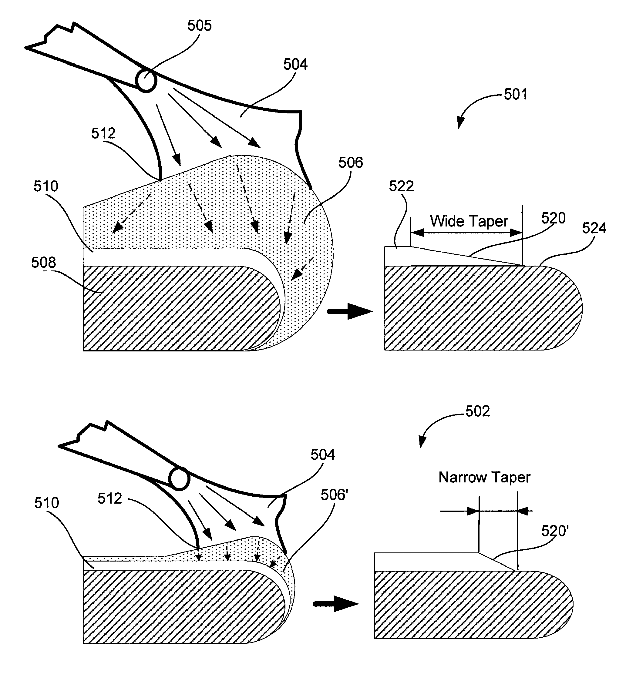
[0079]A standard 300-mm wafer with a 0.5 μm copper bevel edge was provided. The wafer was positioned and aligned in a Novellus Sabre™ system equipped with the deflector shield. The pre-rinse operation was performed using de-ionized water for 2 seconds at 400 rpm. The water was then turned of, and the wafer was accelerated to 600 rpm for another 2 seconds during the wet film thinning operation. In the following operation, the wafer was slowed down to 200 rpm and the etchant including 20% of sulfuric acid and 28% of hydrogen peroxide was applied in two stages. In the first stage, 1 ml of the etchant was delivered at 0.3 ml / sec flow rate. In the second stage, additional 3 ml of the etchant was delivered at 0.15 ml / sec. The overall etching ...


PUM

PropertyMeasurementUnit
widthaaaaaaaaaa
widthaaaaaaaaaa
radiusaaaaaaaaaa

Abstract

Chemical etching methods and associated modules for performing the removal of metal from the edge bevel region of a semiconductor wafer are described. The methods and systems provide the thin layer of pre-rinsing liquid before applying etchant at the edge bevel region of the wafer. The etchant is less diluted and diffuses faster through a thinned layer of rinsing liquid. An edge bevel removal embodiment involving that is particularly effective at reducing process time, narrowing the metal taper and allowing for subsequent chemical mechanical polishing, is disclosed.

Description

CROSS-REFERENCE TO RELATED APPLICATIONS[0001]This application is related to U.S. patent application Ser. No. 11 / 248,874 naming Mayer et al. as inventors, and titled “EDGE BEVEL REMOVAL OF COPPER FROM SILICON WAFERS.” This patent application, as well as any patents, patent applications and publication referenced are hereby incorporated by reference in their entireties and for all purposes.BACKGROUND OF THE INVENTION[0002]This invention relates to technology for removing unwanted metal from semiconductor wafers. More particularly, it pertains to methods for removing unwanted metal, particularly metal in the edge bevel region, using liquid etchants. The invention also pertains to apparatus for performing such removal.[0003]In a typical copper Damascene process, the formation of the desired conductive routes generally begins with a thin physical vapor deposition (PVD) of the metal, followed by a thicker electrofill layer (which is formed by electroplating). The PVD process is typically ...

Claims


Application Information

Patent Timeline
Patent Type & Authority Applications(United States)
IPC IPC(8): H01L21/306
CPCH01L21/02087H01L21/0209H01L21/32134H01L21/02068H01L21/67745H01L21/68735H01L21/68785H01L21/6708
Inventor GANESAN, KOUSIKGHONGADI, SHANTHINATHMAJID, TARIQLABRIE, AARONMAYER, STEVEN T.
Owner NOVELLUS SYSTEMS
Why Eureka
Try Eureka