GUIDED DIAMETER SiC SUBLIMATION GROWTH WITH MULTI-LAYER GROWTH GUIDE

a growth guide and guide technology, applied in the direction of crystal growth process, separation process, fluid protective, etc., can solve the problems of affecting the performance of devices made from single crystals, dislocation and low-angle grain boundary, and most unwanted defects in the sic substrate, etc., to achieve high thermal conductivity and low thermal conductivity

Active Publication Date: 2010-03-11
II VI DELAWARE INC
View PDF15 Cites 13 Cited by
  • Summary
  • Abstract
  • Description
  • Claims
  • Application Information

AI Technical Summary

Benefits of technology

[0022]A growth guide made of carbon / graphite materials is comprised of an inner layer or sleeve and an outer layer. The inner layer, which faces the growing crystal, is made of high thermal conductivity graphite, while the outer layer is made of a porous carbon material having low thermal conductivity. This combination affects heat transport in the cavity of the guide and makes the temperature on its inner surface higher than that of the growing crystal. As a result, deposition of polycrystalline SiC and attachment of the growing crystal to the guide are avoided or eliminated.
[0023]The growth guide has improved resistance against vapor erosion, which is achieved by fabricating the inner layer of the guide from graphite with low binder content. Stability of the growth guide against erosion is additionally improved by removal of excessive silicon from the vapor. The removal is accomplished by including a silicon “getter” inside the growth crucible. The getter is desirably a carbon material with high chemical affinity for silicon.

Problems solved by technology

The performance of such semiconductor devices is strongly affected by crystalline defects in the substrate and epilayer.
Among the most unwanted defects in the SiC substrate are micropipes, dislocations and low-angle grain boundaries.
It is generally recognized that high defect densities in SiC and GaN single crystals adversely affect the performance of devices made from these single crystals.
However, this technique is too complex and lengthy to be used as an industrial process.
This type of expansion leads to a high degree of thermo-elastic stress and generation of dislocations, especially near the edge of the crystal boule.
Another problem is the formation of polycrystalline SiC deposits on the growth guide, as shown in FIG. 4C.
In the process of growth, the single crystal comes in contact with the guide, attaches to it and develops crude defects at the edge.
This makes the accuracy of thermal modeling low.
Removal of the graphitized binder liberates microscopic graphite grains, which may become airborne and contaminate the growing SiC crystal.
This makes graphite with high binder content more prone to gas / vapor erosion than graphite with low binder content.
However, in the conditions of SiC sublimation growth, these refractory coatings are not inert.
Rather, they react with the vapor, peel off and lead to crystal contamination.

Method used


Image

  • GUIDED DIAMETER SiC SUBLIMATION GROWTH WITH MULTI-LAYER GROWTH GUIDE
  • GUIDED DIAMETER SiC SUBLIMATION GROWTH WITH MULTI-LAYER GROWTH GUIDE
  • GUIDED DIAMETER SiC SUBLIMATION GROWTH WITH MULTI-LAYER GROWTH GUIDE

Examples


Embodiment Construction

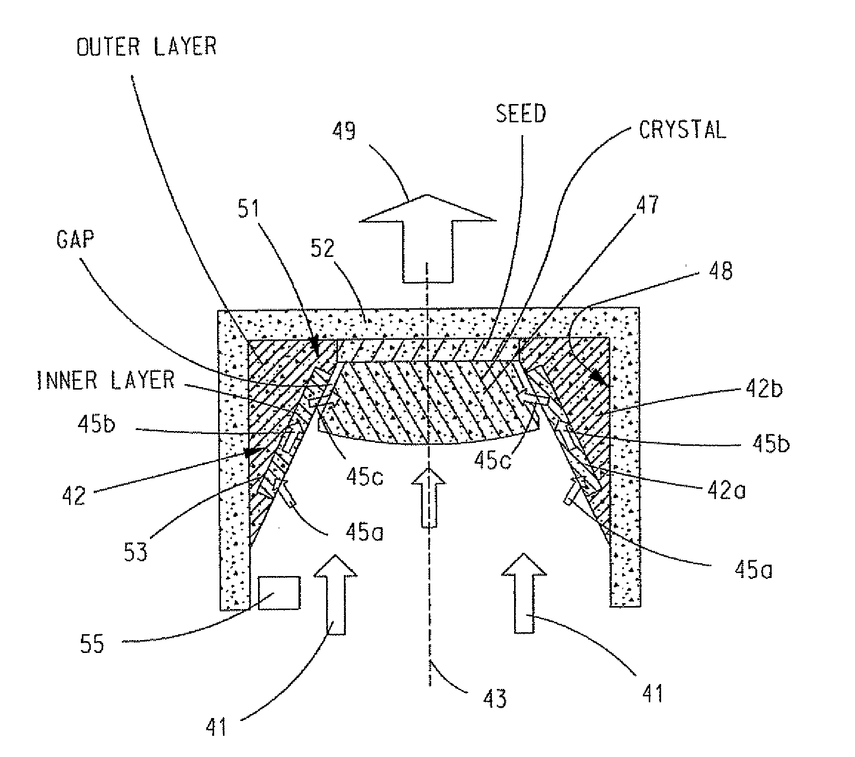
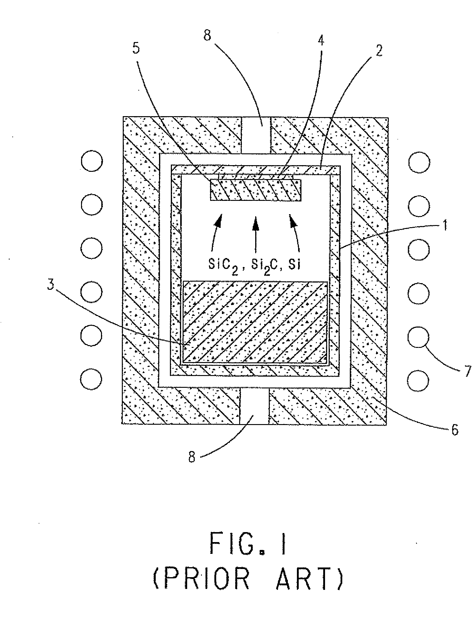
[0052]The SiC sublimation crystal growth disclosed herein utilizes guided expansion of the crystal diameter during the growth thereof to eliminate or avoid erosion of the growth guide, deposition of polycrystalline SiC on the guide and attachment of the crystal to the guide. It can be used for the production of large-diameter, high-quality SiC single crystals.

[0053]To understand the effect of the growth guide design on the temperature of its inner surface and its correlation with the crystal temperature, reference will now be made to FIGS. 5A, 5B and 6. FIGS. 5A, 5B and 6 each show schematically the upper part of a SiC crystal growth crucible, like crucible 1 in FIG. 1, with a thermally nonconductive conical growth guide, a thermally conductive conical growth guide and a multi-layer growth guide in accordance with an embodiment of the present invention, respectively. Each growth guide is disposed at the crucible top and surrounds the SiC seed crystal and the growing SiC crystal boul...


PUM

PropertyMeasurementUnit
angleaaaaaaaaaa
angleaaaaaaaaaa
angleaaaaaaaaaa

Abstract

In the growth of a SiC boule, a growth guide is provided inside of a growth crucible that is charged with SiC source material at a bottom of the crucible and a SiC seed crystal at a top of the crucible. The growth guide has an inner layer that defines at least part of an opening in the growth guide and an outer layer that supports the inner layer in the crucible. The opening faces the source material with the seed crystal positioned at an end of the opening opposite the source material. The inner layer is formed from a first material having a higher thermal conductivity than the second, different material forming the outer layer. The source material is sublimation grown on the seed crystal in the growth crucible via the opening in the growth guide to thereby form the SiC boule on the seed crystal.

Description

BACKGROUND OF THE INVENTION[0001]Wafers of silicon carbide of 4H and 6H polytypes serve as lattice-matched substrates to grow epitaxial layers of SiC and GaN which are used for fabrication of SiC- and GaN-based semiconductor devices. The performance of such semiconductor devices is strongly affected by crystalline defects in the substrate and epilayer. Among the most unwanted defects in the SiC substrate are micropipes, dislocations and low-angle grain boundaries. It is generally recognized that high defect densities in SiC and GaN single crystals adversely affect the performance of devices made from these single crystals.[0002]With reference to FIG. 1, large SiC single crystals are commonly grown by a sublimation technique called Physical Vapor Transport (PVT). A typical PVT growth system includes a crucible 1, typically made of graphite, loaded with polycrystalline SiC source material 3 and a SiC seed crystal 4, typically, a SiC single crystal. Source 3 is disposed at the bottom o...

Claims


Application Information

Patent Timeline
Patent Type & Authority Applications(United States)
IPC IPC(8): C01B31/36B01D9/00
CPCC30B23/005C30B35/00C30B29/36
Inventor ZWIEBACK, ILYAGUPTA, AVINASH K.SEMENAS, EDWARDANDERSON, THOMAS E.
Owner II VI DELAWARE INC
Why Eureka
Try Eureka