Application specific solar cell and method for manufacture using thin film photovoltaic materials

a technology of photovoltaic materials and solar cells, applied in the field of photovoltaic materials, can solve the problems of wasting energy, reducing the efficiency of solar energy conversion, and reducing the efficiency of sunlight conversion into electrical power, so as to achieve easy control and automation of laser beam scanning operations, and improve the efficiency of sunlight conversion. , the effect of increasing the efficiency of sunlight conversion

US20100062560A1Active Publication Date: 2010-03-11CM MFG
27 Cites 31 Cited by

Patent Information

Authority / Receiving Office
US · United States
Patent Type
Applications(United States)
Current Assignee / Owner
Publication Date
2010-03-11

Smart Images

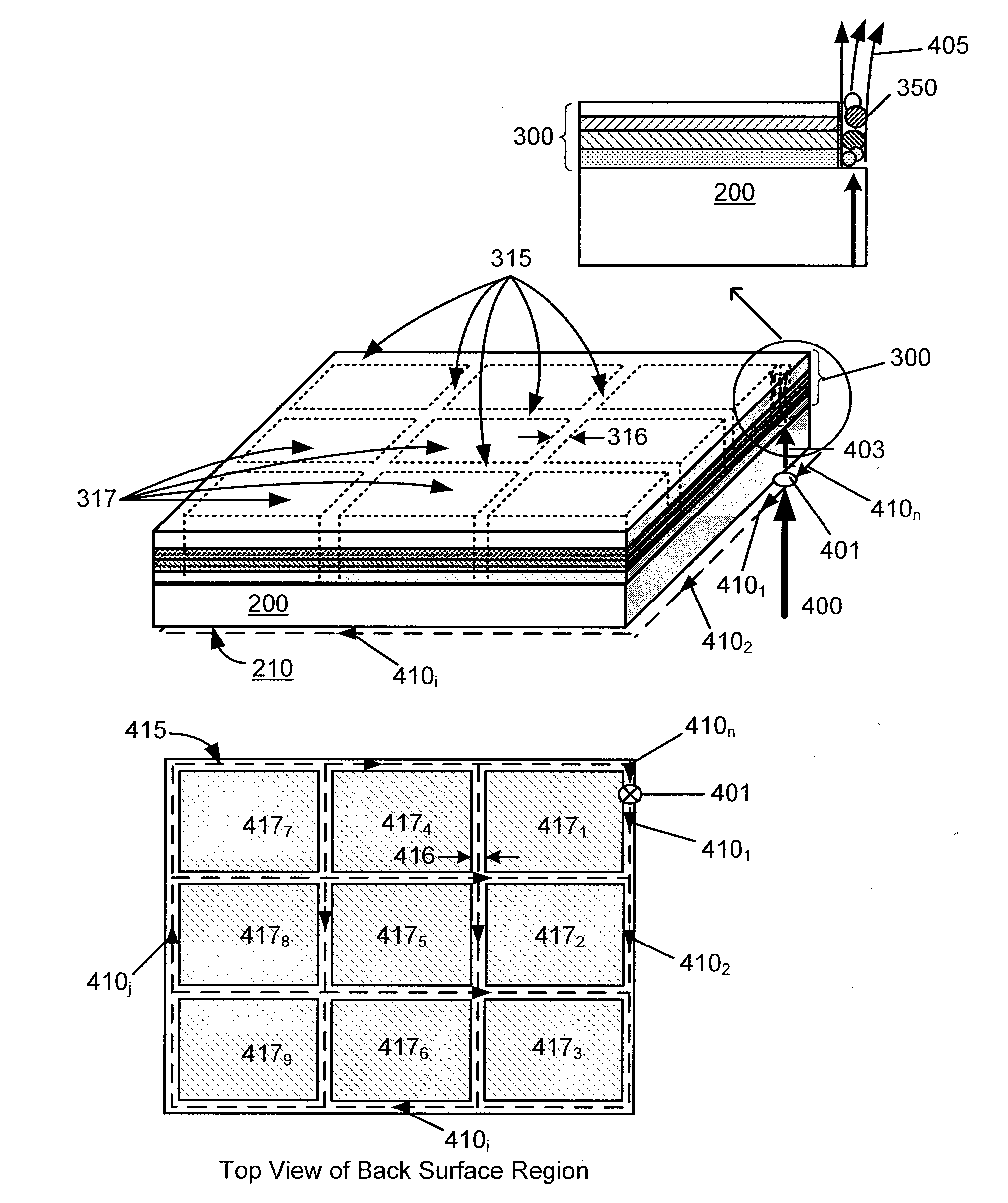
  • Figure 1
    Figure 1
  • Figure 2
    Figure 2
  • Figure 3
    Figure 3
Patent Text Reader

Abstract

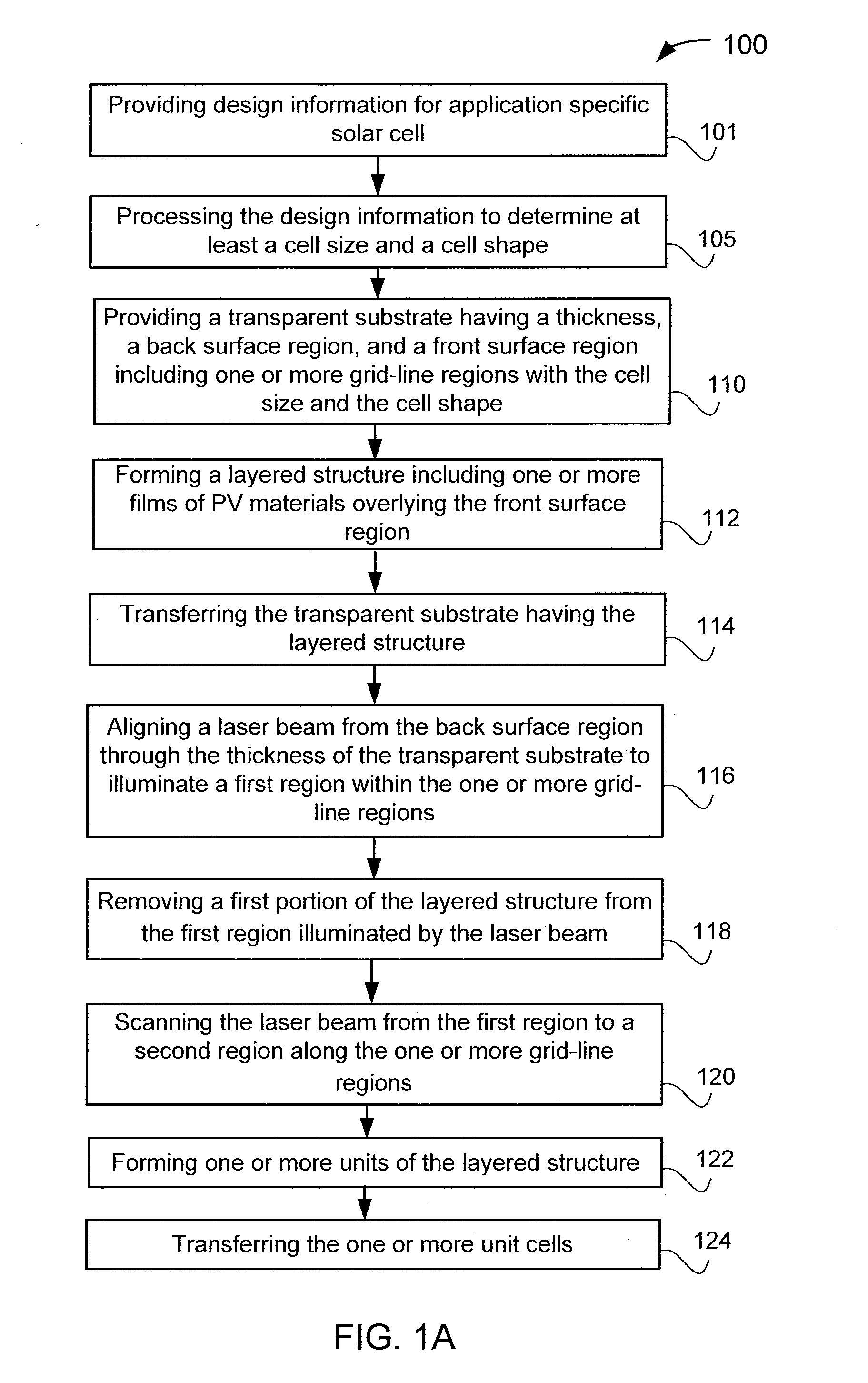
A method for manufacture of application specific solar cells includes providing and processing custom design information to determine at least a cell size and a cell shape. The method includes providing a transparent substrate having a back surface region, a front surface region, and one or more grid-line regions overlying the front side surface region. The one or more grid regions provide one or more unit cells having the cell size and the cell shape. The method further includes forming a layered structure including photovoltaic materials overlying the front surface region. Additionally, the method includes aligning a laser beam from the back surface region to illuminate a first region within the one or more grid-line regions, subjecting a first portion of the layered structure overlying the first region to the laser beam to separate the first portion of the layered structure from the first region, and scanning the laser beam along the one or more grid-line regions to cause formation of one or more unit cells having the cell size and cell shape. The method further includes transferring the one or more unit cells.
Need to check novelty before this filing date? Find Prior Art

Description

CROSS-REFERENCES TO RELATED APPLICATIONS

[0001] This application claims priority to U.S. Provisional Patent Application No. 61 / 095,939, filed Sep. 10, 2008, entitled “APPLICATION SPECIFIC SOLAR CELL AND METHOD FOR MANUFACTURE USING THIN FILM PHOTOVOLTAIC MATERIALS” by inventors Chester A. Farris, III and Albert S. Brown, commonly assigned and incorporated by reference herein for all purposes.BACKGROUND OF THE INVENTION

[0002] The present invention relates generally to photovoltaic materials. More particularly, the present invention provides a method and system for design and manufacture of a solar module using a laser separation process for forming one or more unit cells from continuous layered structure of photovoltaic materials. Merely by way of example, the present method and structure have been implemented to an application specific thin film solar cell having single or multi-junction photovoltaic materials, but it would be recognized that the invention may have other configurations...

Examples

Embodiment Construction

[0023]The present invention relates generally to photovoltaic materials. More particularly, the present invention provides a method and system for design and manufacture of a solar module using a laser separation process for forming one or more unit cells from continuous layered structure of photovoltaic materials. Merely by way of example, the present method and structure have been implemented to manufacture an application specific thin film solar cell having single or multi junction photovoltaic materials, but it would be recognized that the invention may have other configurations.

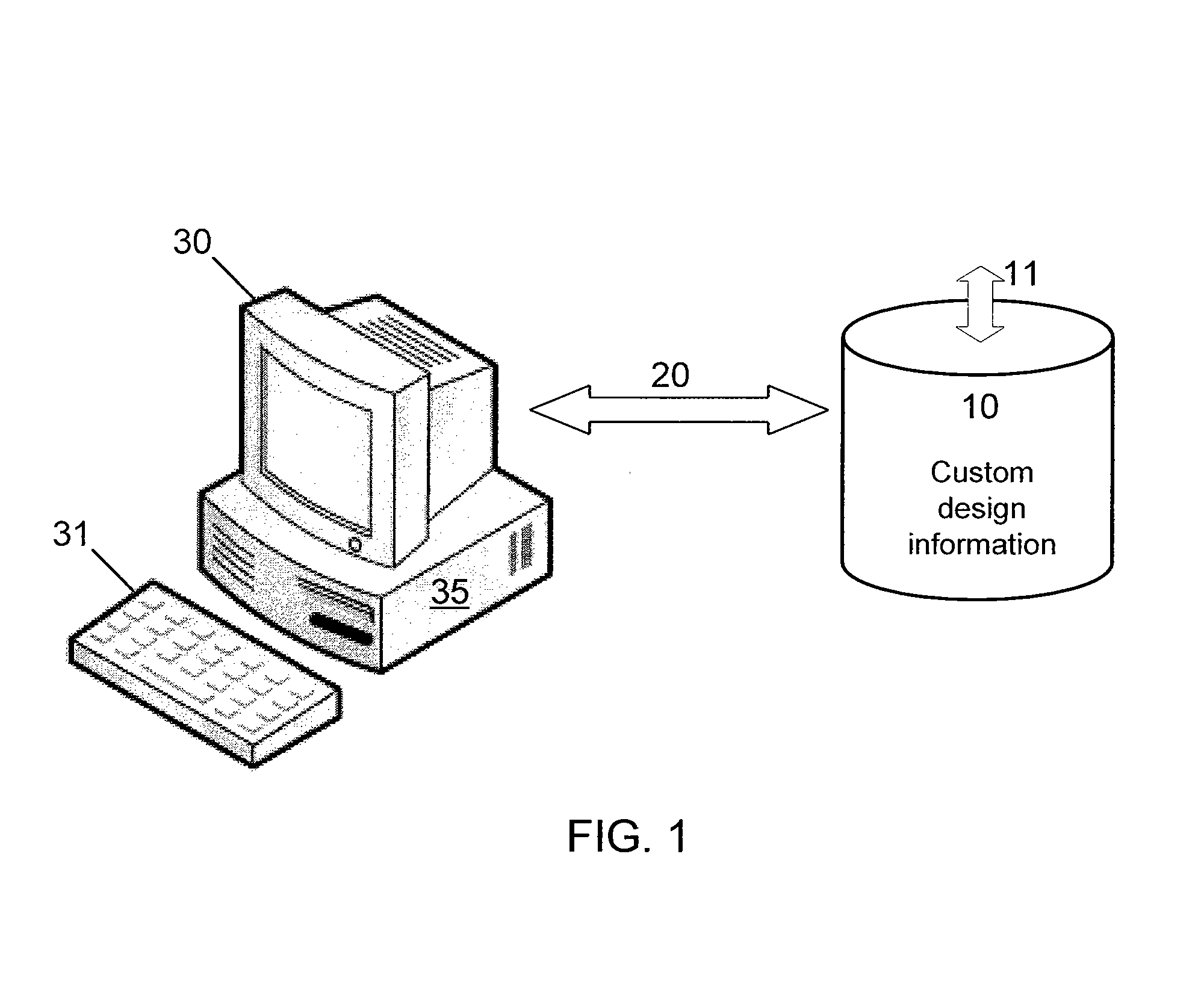
[0024]FIG. 1 is a simplified diagram illustrating a computer configured to receive a custom design information stored in a database according to an embodiment of the present invention. This diagram is merely an example, which should not unduly limit the scope of the claims herein. As shown, a database 10 is established for storing a plurality of custom design information data. In one embodiment, the data...