Platinum silicide tip apices for probe-based technologies

a technology of tip apex conductivity and silicide, which is applied in the field of probe-based technologies, can solve the problems of c-afm, reducing the reliability and reducing the accuracy of nano-scale tip apex conductivity

Active Publication Date: 2010-03-25
IBM CORP
View PDF26 Cites 6 Cited by
  • Summary
  • Abstract
  • Description
  • Claims
  • Application Information

AI Technical Summary

Problems solved by technology

Existing probes for conducting-mode atomic force microscopy (C-AFM) have disadvantages typically associated with wear of the conductive coating.
However, this renders the processes difficult to scale, in particular for use on applications such as nanotechnology-based probe storage.
However, as with most c-AFM measurements, the reliability of the nanoscale tip apex conductivity, especially at the tip-sample interface, is a serious concern in commercialization.
This coating can wear off quickly, given the high forces required for reliable conduction.
However, their costs are prohibitive for any large-scale array fabrication as required for probe storage, probe-based manufacturing and other applications that require one or more probes at low cost.
However, use of TiSi for conduction by forming TiSi on a silicon wafer results in an oxide forming on the surface (as evidenced by the presence of the breakdown voltage), which impeded conduction.

Method used


Image

  • Platinum silicide tip apices for probe-based technologies
  • Platinum silicide tip apices for probe-based technologies
  • Platinum silicide tip apices for probe-based technologies

Examples


Embodiment Construction

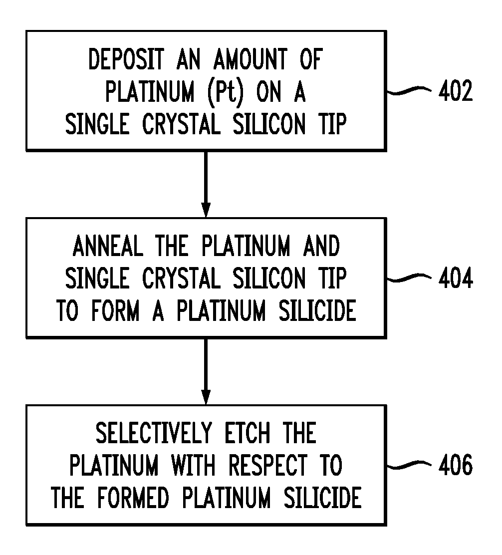
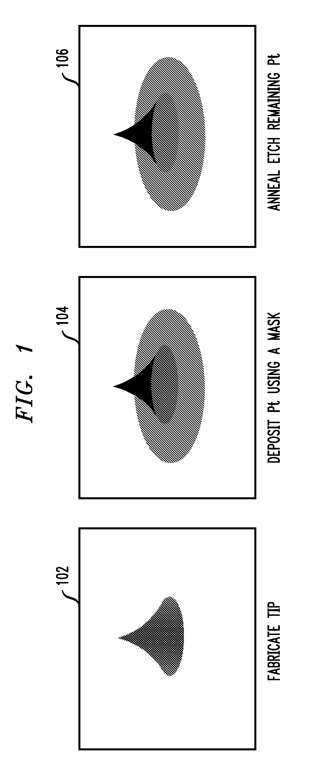
[0014]Principles of the present invention include platinum silicide tip apices for applications of all types of probe-based technologies for superior conduction and / or wear resistance. One or more embodiments of the invention include forming silicides of platinum (for example, PtSi and / or Pt2Si) at the tip apex. Silicides of platinum as tip apex material provide hardness and its known properties in both preventing oxide formation and reducing the Schottky barrier. Additionally, silicides of platinum are an ohmic contact to Si, which is useful for good conduction. Platinum (Pt) is also a noble metal, and therefore reduces probability of oxide at the tip. Further, silicides of platinum can be easily formed only at the tip by a single mask layer, and this process is completely compatible with standard micro-electro-mechanical systems (MEMS) processing. Silicides of platinum can also readily be incorporated into the cantilever fabrication process using a lift-off and annealing step.

[001...


PUM

PropertyMeasurementUnit
apex radiusaaaaaaaaaa
linear velocityaaaaaaaaaa
total sliding distanceaaaaaaaaaa

Abstract

Tips including a platinum silicide at an apex of a single crystal silicon tip are provided herein. Also, techniques for creating a tip are provided. The techniques include depositing an amount of platinum (Pt) on a single crystal silicon tip, annealing the platinum and single crystal silicon tip to form a platinum silicide, and selectively etching the platinum with respect to the formed platinum silicide.

Description

FIELD OF THE INVENTION[0001]The present invention generally relates to probe-based technologies, and, more particularly, to tip apices.BACKGROUND OF THE INVENTION[0002]Existing probes for conducting-mode atomic force microscopy (C-AFM) have disadvantages typically associated with wear of the conductive coating. For this reason, monolithic probes of metals are sometimes used, especially for long-term C-AFM experiments. However, this renders the processes difficult to scale, in particular for use on applications such as nanotechnology-based probe storage.[0003]Existing approaches can also include electrical probe storage based on Joule heating in phase-change media, which has potential for high data rates at low cost. The phase-change medium typically used in such storage systems is the Ge2Sb2Te5 (from the chalcogenide family, commonly referred to as GST). To write bits, Joule heating of the medium by passing a current through a conducting cantilever with a nanometric tip is typically...

Claims


Application Information

Patent Timeline
Patent Type & Authority Applications(United States)
IPC IPC(8): G01N13/16
CPCG01Q60/40B82Y35/00
Inventor BHASKARAN, HARISHDESPONT, MICHELDRECHSLER, UTESEBASTIAN, ABU
Owner IBM CORP
Why Eureka
Try Eureka