
Flow Sensor and Method of Fabrication

a flow sensor and flow sensor technology, applied in the field of flow sensors, can solve the problems that the device designer would normally be drawn away from the use of self-supporting silicon structures in heat carrying elements by the device designer, and achieve the effects of reducing the overall sensor size, enhancing media compatibility, and eliminating the damage to exposed wire bonds

Inactive Publication Date: 2010-04-01
FLOWMEMS
View PDF27 Cites 42 Cited by
  • Summary
  • Abstract
  • Description
  • Claims
  • Application Information

AI Technical Summary

Benefits of technology

[0007]The present invention provides a flow sensor that can exhibit at least one of higher measurement sensitivity, wider operating temperature range, and improved media compatibility, as compared to the prior-art. In some embodiments, flow sensors in accordance with the present invention comprise a heater and a temperature sensor, each of which is self-supported over a cavity formed in a substrate.
[0008]The present invention is enabled by the recognition that the benefits of using single-crystal silicon as the primary structural component for heat carrying elements, such as heater elements and temperature sensing elements, outweigh the negatives a device designer would normally associate with its use in this capacity. Specifically, single-crystal silicon structures that are thick enough to be self-supporting and are characterized by a relatively low electrical resistance per unit length have a high thermal conductance. Due to these perceived limitations, a device designer would normally be drawn away from the use of self-supported silicon structures in heat carrying elements. The inventors, however, recognized that single-crystal structures of sufficient thickness would obviate the need for a membrane to support the heater and temperature sensors above a substrate, which is typically required in prior-art devices. Since embodiments of the present invention do not include such a membrane, undesired heat dissipation due to thermal conductance in the membrane is eliminated. In addition, for single-crystal structures of suitable thickness: (i) the overall thermal efficiency of such elements can be improved over comparable prior art devices; and (ii) sensor sensitivity can be increased due to the fact that heat dissipation from a heater to a temperature sensor through the membrane is eliminated.
[0009]Some embodiments of the present invention comprise one or more self-supported structures, such as a heater element and / or temperature sensor, wherein each self-supported structure comprises a portion that is disposed over a cavity formed in the substrate. The presence of the cavity mitigates or eliminates significant heat conduction from the suspended portion into the substrate material. Each self-supported structure comprises a central core of single-crystal silicon that is surrounded by a dielectric material, an arrangement that mitigates or eliminates deformation of device elements over the sensor operating temperature range due to bi-material effects, a common problem in prior art. In some embodiments, the dielectric material:
[0011]ii. enhances the mechanical strength of the self-supported device elements; or
[0014]Some embodiments of the present invention comprise a silicon-on-insulator substrate having one or more through-substrate contacts. These through-substrate contacts enable electrical connectivity between backside contacts and thermal device elements formed in the active layer of the silicon-on-insulator substrate. In some embodiments, through-substrate contacts enable the elimination of metal wire bond pads and wire bonds from the front-side surface. As a result, damage to exposed wire bonds by media flow is eliminated. Further, media compatibility is enhanced and overall sensor size can be reduced.

Problems solved by technology

Due to these perceived limitations, a device designer would normally be drawn away from the use of self-supported silicon structures in heat carrying elements.

Method used


Image

  • Flow Sensor and Method of Fabrication
  • Flow Sensor and Method of Fabrication
  • Flow Sensor and Method of Fabrication

Examples


Embodiment Construction

[0033]The following terms are defined for use in this Specification, including the appended claims:[0034]Single-crystal material means material having a crystalline structure that comprises substantially only one type of unit-cell. A single-crystal layer, however, may exhibit some crystalline defects such as stacking faults, dislocations, or other commonly occurring crystalline defects. Examples of single-crystal materials include, without limitation, single-crystal silicon, single-crystal germanium, single-crystal III-V semiconductors and their compounds, and single-crystal silicon carbide.

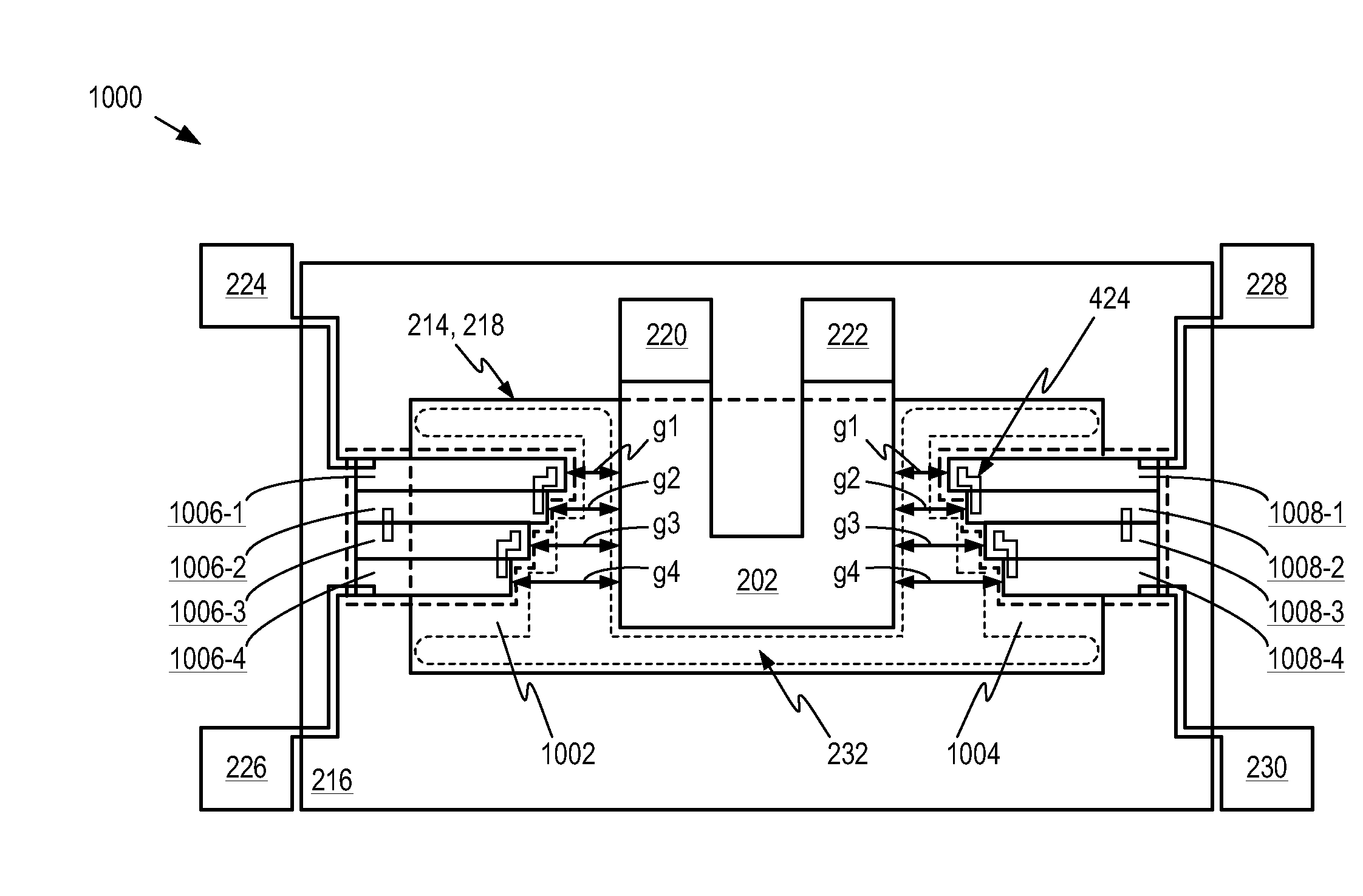
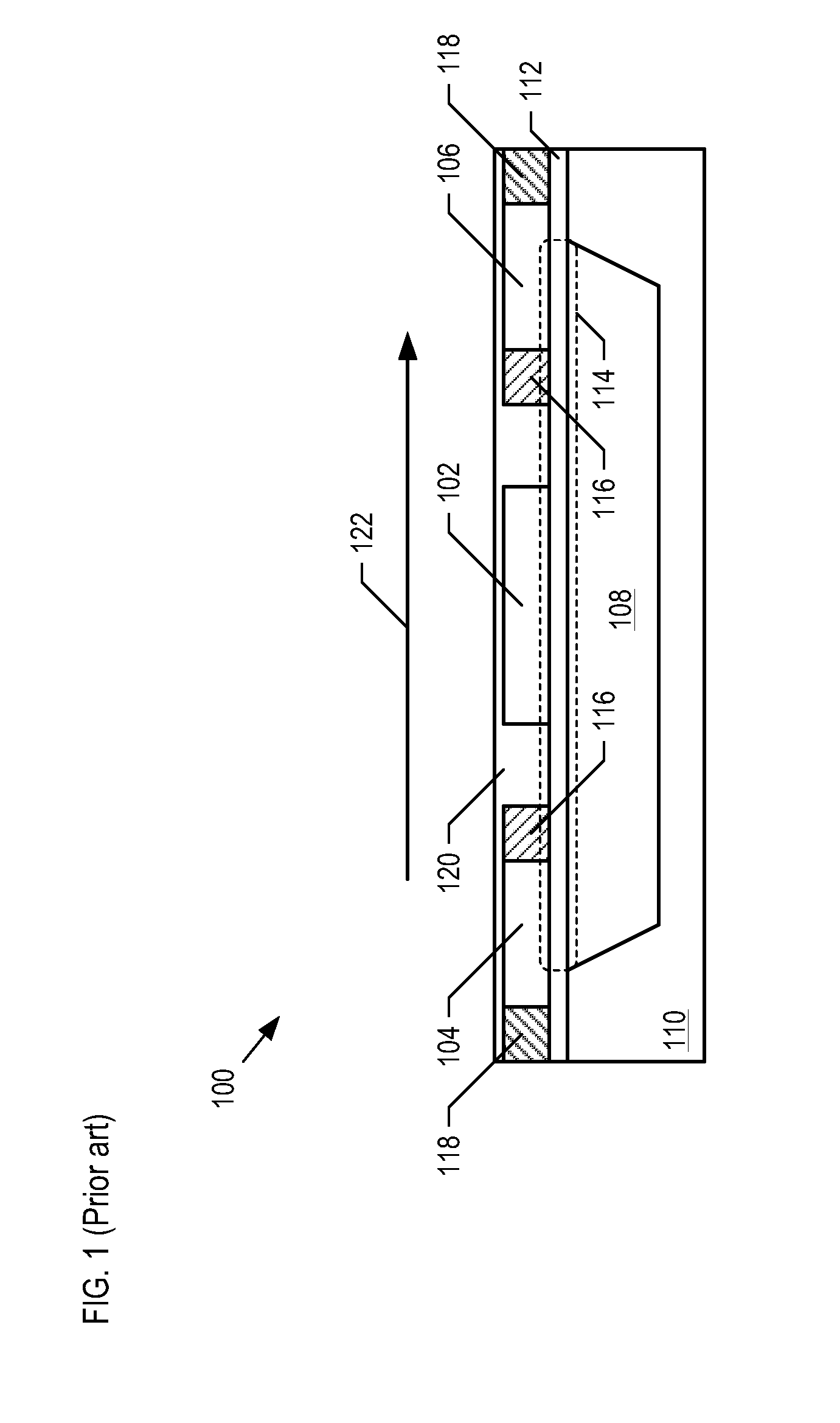
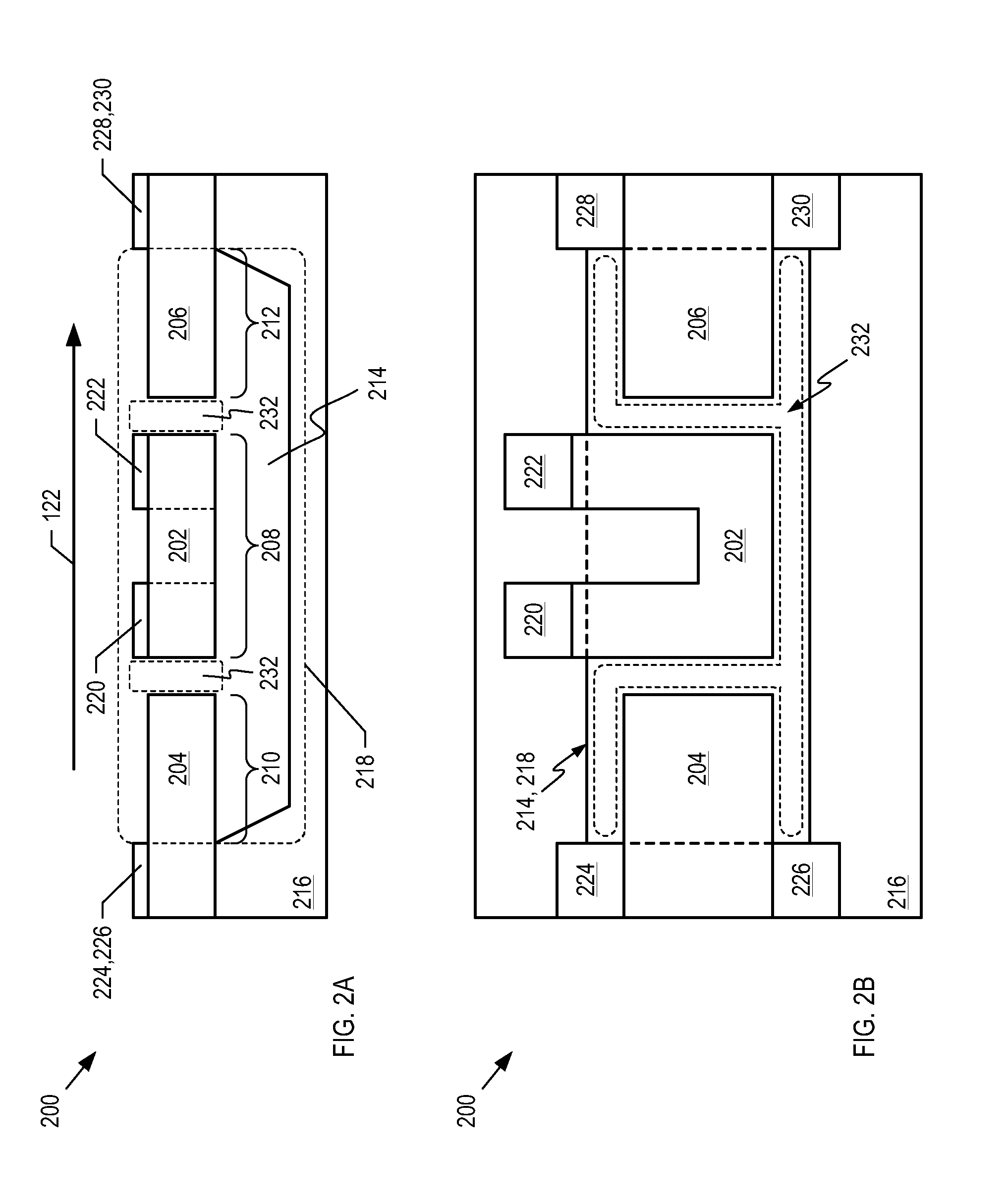
[0035]FIG. 1 depicts a cross-sectional view of a schematic diagram of a portion of a flow sensor in accordance with the prior-art. Flow sensor 100 comprises heater 102, temperature sensors 104 and 106, membrane 114, and substrate 110. Exemplary prior-art flow sensors are disclosed in U.S. Pat. No. 4,478,076, issued Oct. 23, 1984 and U.S. Pat. No. 6,871,538, issued Mar. 29, 2005.

[0036]Heater 102 i...


PUM


Abstract

A method for forming a flow sensor having self-supported heat-carrying elements is disclosed. Self-supported heat-carrying elements are capable of operating with higher thermal efficiency, enabling lower power consumption and higher sensitivity, due to a lack of heat loss into a supporting membrane. Self-supported heat-carrying elements facilitate wider operating temperature range and compatibility with harsh media.

Description

FIELD OF THE INVENTION[0001]The present invention relates to sensors in general, and, more particularly, to flow sensors.BACKGROUND OF THE INVENTION[0002]The ability to accurately measure fluid flow, such as air flow, is becoming more important, particularly as the need for energy efficiency has become critical in many applications. Many approaches of different complexities have been used in the prior-art to form flow sensors in the prior art—from simple resistance-based sensors to fully integrated micro-electro-mechanical (MEMS) systems.[0003]The simplest flow sensors comprise a single hot wire or thermistor that is mounted on the end of a probe, which is inserted into a flow stream. A temperature drop in response to the presence of fluid flow causes a change in the resistance of the hot wire or thermistor.[0004]Improved flow sensors were enabled by the monolithic integration of heaters and temperature sensors on a common silicon substrate. A typical conventional flow sensor compri...

Claims


Application Information

Patent Timeline
IPC IPC(8): H01L21/28H01L29/66
CPCG01F1/6888G01F1/6845
Inventor MEHREGANY, MEHRANVANDELLI, JR., NELSIMAR MOURA
Owner FLOWMEMS
Learn More