

Inductance element, method for manufacturing the same, and switching power supply using the same
a technology of inductance elements and manufacturing methods, applied in the field of inductance elements, can solve the problems of power supply noise, various types of electronic equipment malfunction, and degradation of magnetic characteristics, and achieve the effect of suppressing the degradation of magnetic characteristics and improving mass productivity
- Summary
- Abstract
- Description
- Claims
- Application Information
AI Technical Summary
Benefits of technology
Problems solved by technology
Method used
Image

Examples
examples
[0067]Specific examples of the present invention and the evaluated results are described below.
examples 1 to 6
, Comparative Examples 1 to 2
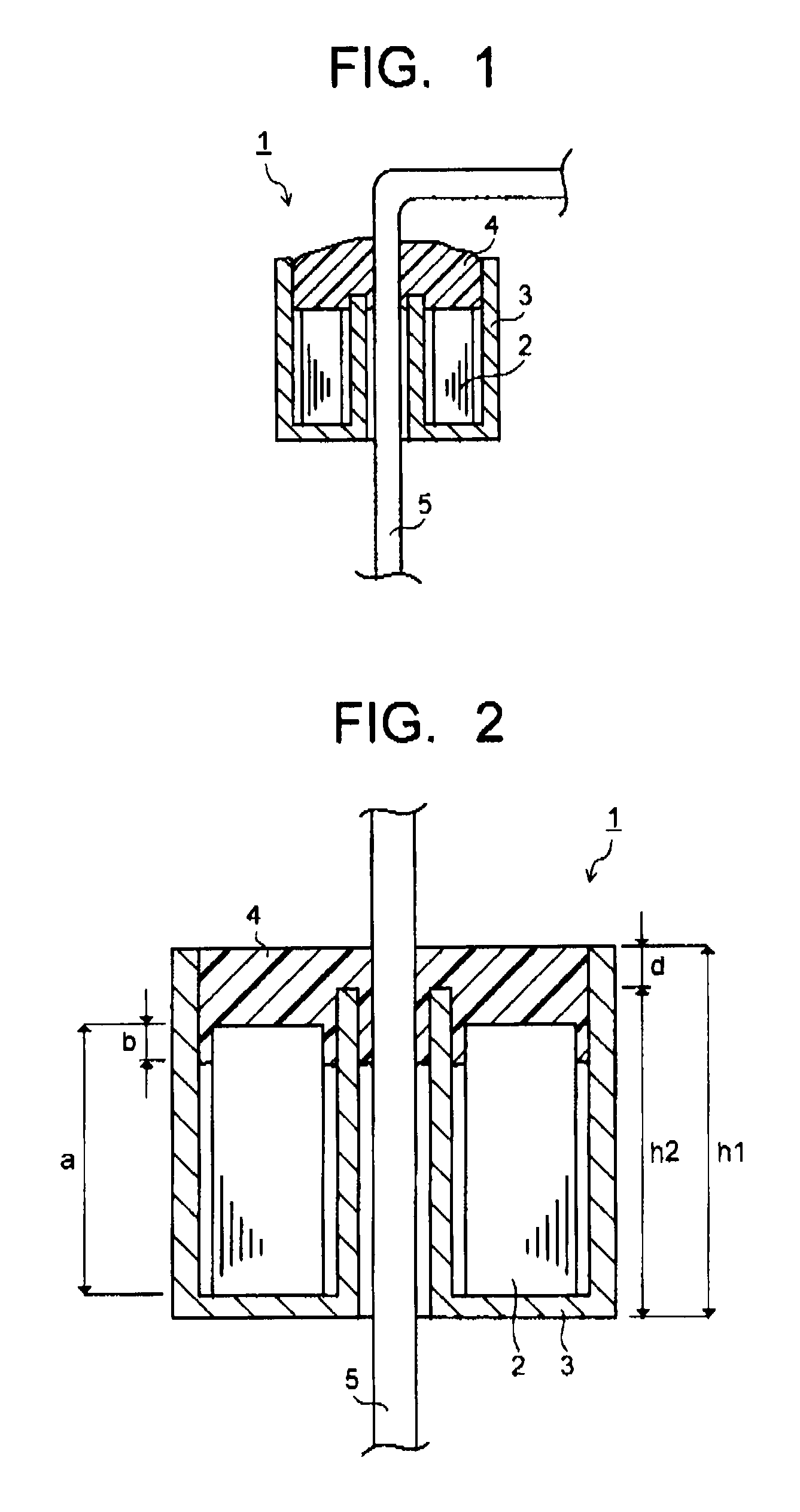
[0068]An amorphous magnetic alloy ribbon (thickness of 18 Ka) having a composition of (Co0.94Fe0.05Cr0.01)72Si15B13 was wound to form a doughnut-shaped magnetic core (toroidal core). An insulation coating was previously formed on a surface of the magnetic ribbon. The doughnut-shaped magnetic core was determined to have an outer diameter of 3 mm, an inner diameter of 2 mm and a height of 3 mm.
[0069]The doughnut-shaped magnetic core was then housed in a PBT bottomed container (outer diameter 3.4 mm, inner diameter 1.6 mm, height 4.5 mm, thickness 0.1 mm). The bottomed container was determined to have [height of outer wall portion 4.5 mm-height of inner wall portion 3.2 mm=1.3 mm]. Then, a conductive lead wire having a diameter of 0.8 mm undergone bending processing was inserted, and the magnetic core, the container and the lead portion were integrally fixed by using an acryl modified silicone resin-based adhesive. The penetration ratio of the adhesive port...
examples 7 to 10
[0073]The inductance element of Example 2 was used with the ratio of the adhesive portion penetrating into the magnetic core varied to prepare inductance elements, and the same measurement was conducted. The results are shown in Table 2.
TABLE 2Penetration ratioChange rate ofof adhesiveValue Lvalue L after 1000portion (%)(μH)hours (%)Example 754.810 to 30% downExample 8104.710 to 30% downExample 9304.710 to 30% downExample 10504.615 to 35% down
[0074]As shown in Table 2, when the penetration ratio of the adhesive portion into the gap of the magnetic core exceeds 30%, the magnetic characteristics might be decreased.
PUM
| Property | Measurement | Unit |
|---|---|---|
| temperature | aaaaa | aaaaa |
| thickness | aaaaa | aaaaa |
| grain diameter | aaaaa | aaaaa |
Abstract
Description
Claims
Application Information