Optical connecting apparatus

a technology of optical connection and connecting apparatus, which is applied in the direction of multiplex communication, instruments, optical elements, etc., can solve the problems of increasing transmission loss, preventing an increase in capability, and circuits becoming complex, so as to achieve stable optical connection and mitigate the effect of heat from the integrated circuit to the signal conversion section

Active Publication Date: 2010-04-29
NEC CORP
View PDF6 Cites 5 Cited by
  • Summary
  • Abstract
  • Description
  • Claims
  • Application Information

AI Technical Summary

Benefits of technology

[0022]According to the present invention, while it is possible to implement high-density optical wiring nearby integrated circuits, it is possible to locate the signal conversion section away from the optical transmit section and the optical receive section on which the integrated circuits are mounted. Therefore, the effect of heat from the integrated circuits to the signal conversion section can be mitigated, thereby optical connection can be stable.

Problems solved by technology

However, while the degree of integration increases, the density of LSI package's signal pins which input and output signals does not increase, thereby preventing an increase in capability.
The increased speed, however, cause various problems.
For example, transmission loss increases due to skin effect on the lines of a circuit board.
As a result, problems that circuits become complex and power consumption increases are brought.

Method used


Image

  • Optical connecting apparatus
  • Optical connecting apparatus
  • Optical connecting apparatus

Examples


Embodiment Construction

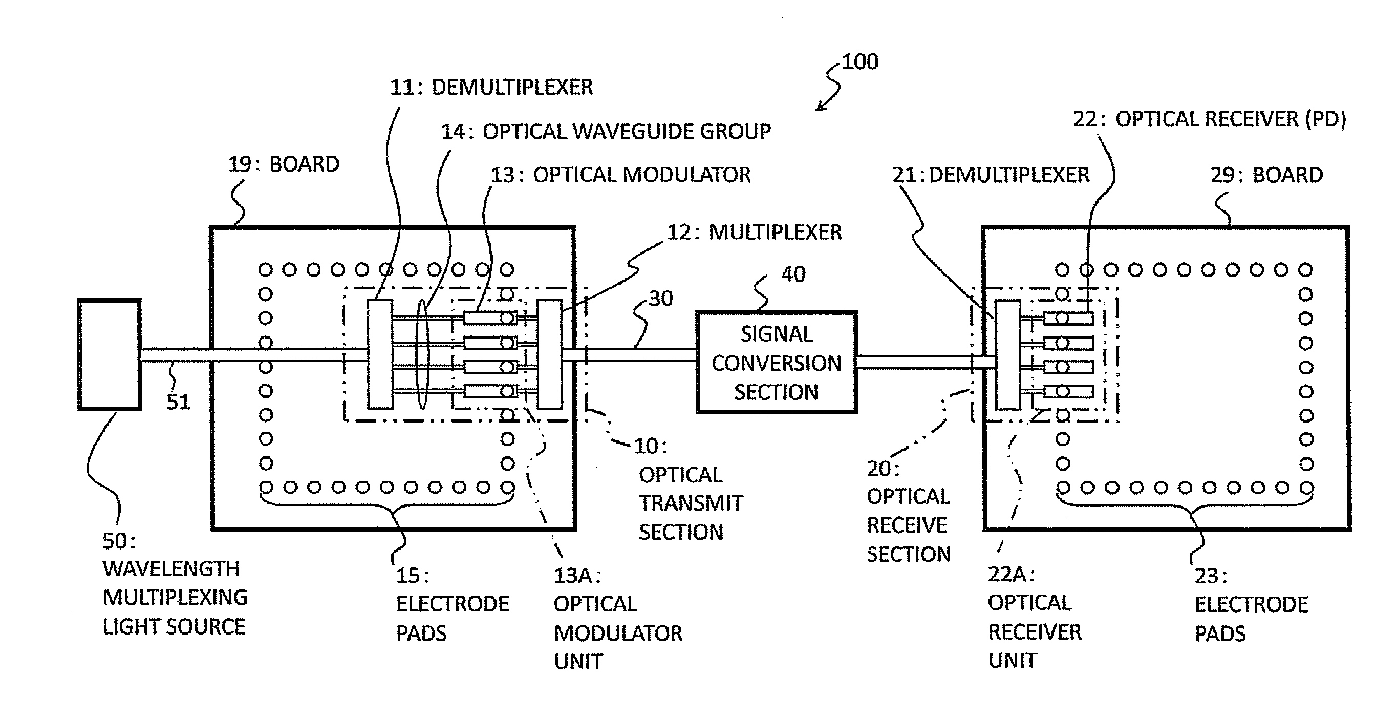
[0045]FIG. 1 shows the configuration of an optical connecting apparatus 100 according to an embodiment of the present invention. The optical connecting apparatus 100 includes a wavelength multiplexing light source 50 which outputs optical beams the wavelengths of which respectively correspond to a plurality of transmission channels; an optical transmit section 10 which is formed on a board 19; an optical receive section 20 which is formed on a board 29; and a signal conversion section 40 which is inlet in an optical wiring section 30. The optical wiring section 30 provides an optical line of a single system between the optical transmit section 10 and the optical receive section 20. The optical wiring section 30 may consist of an optical fiber or an optical waveguide.

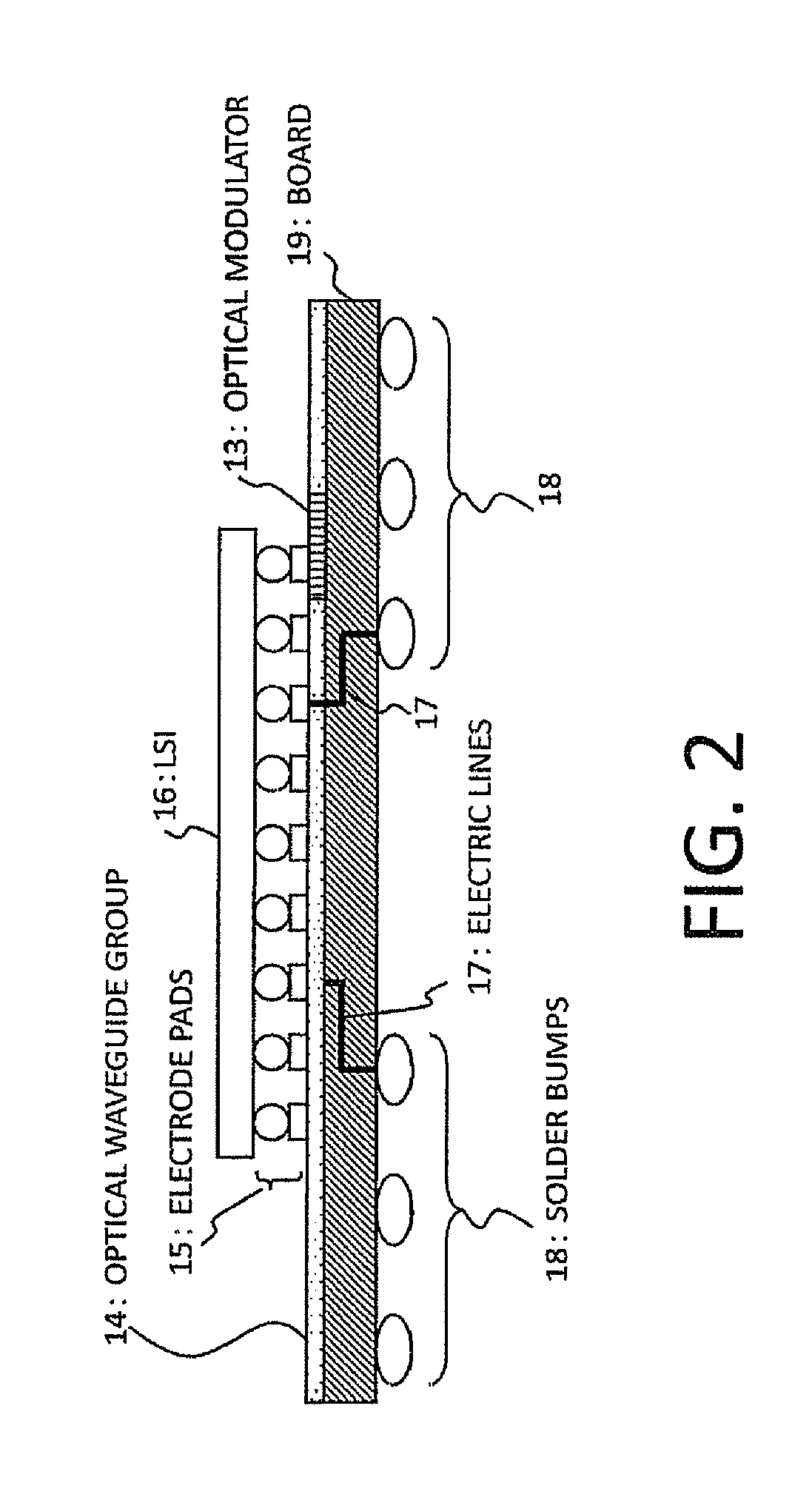
[0046]LSIs (not shown in FIG. 1) that output single-frequency signals are respectively mounted on the boards 19 and 29. The LSIs are electrically connected to the boards (19 and 29) through electrode pads 15 and electrod...


PUM


Abstract

An optical connecting apparatus has a light source outputting an optical signal indicating a plurality of wavelengths which correspond to a plurality of transmission channels, an optical transmit section and an optical receive section being mounted with integrated circuits and being connected to each other through an optical line of a single system, and a signal conversion section being inlet in the optical line and converting a phase modulated signal into an intensity modulated signal. The optical transmit section includes: a demultiplexer which separates the optical signal from the light source according to the transmission channels; an optical modulator unit which generates phase modulated signals by implementing phase modulation with optical signals from the demultiplexer by using a plurality of optical modulators whose operations are synchronized by a signal from the integrated circuit; and a multiplexer which multiplexes the phase modulated signals from the optical modulator unit and outputs the multiplexed phase modulated signals to the signal conversion section through the optical line. The optical receive section includes: a demultiplexer which separates the intensity modulated signal from the signal conversion section according to the transmission channels; and an optical receiver unit which converts the intensity modulated signals from the demultiplexer into electric signals.

Description

TECHNICAL FIELD[0001]The present invention relates to an optical connecting apparatus for connection of many signals such as a signal transmitting device between LSIs and a backplane of a device.BACKGROUND ART[0002]In an advanced information society, there is a demand for the increased capabilities of an information processing device such as a server and a network device such as a router. To meet this demand, it is considered effective to miniaturize LSIs to increase the degree of integration and the degree of integration is expected to steadily increase in the future.[0003]However, while the degree of integration increases, the density of LSI package's signal pins which input and output signals does not increase, thereby preventing an increase in capability. The problem is a so-called “pin bottleneck.”[0004]To solve the above-mentioned pin bottleneck, an attempt is being made to increase the speed of transmitting signals per pin by multiplexing a plurality of signals (parallel-to-s...

Claims


Application Information

Patent Timeline
Patent Type & Authority Applications(United States)
IPC IPC(8): H04J14/02H04B10/50H04B10/516H04B10/67
CPCH04B10/505H04B10/516H04J14/02H04B2210/517H04B10/675H01L2224/16225H01L2924/15311
Inventor OGURA, ICHIRO
Owner NEC CORP
Why Eureka
Try Eureka