
Copper-gallium allay sputtering target, method for fabricating the same and related applications

a sputtering target and copper gallium allay technology, applied in the direction of diaphragms, metallic material coating processes, electrical equipment, etc., can solve the problems of increasing the cost of sputtering target production, difficult to be sintered, macro segregation or micro segregation, etc., to achieve the effect of improving quality and properties

Inactive Publication Date: 2010-05-13
SOLAR APPLIED MATERIALS TECHNOLOGY CORPORATION
View PDF5 Cites 39 Cited by
  • Summary
  • Abstract
  • Description
  • Claims
  • Application Information

AI Technical Summary

Benefits of technology

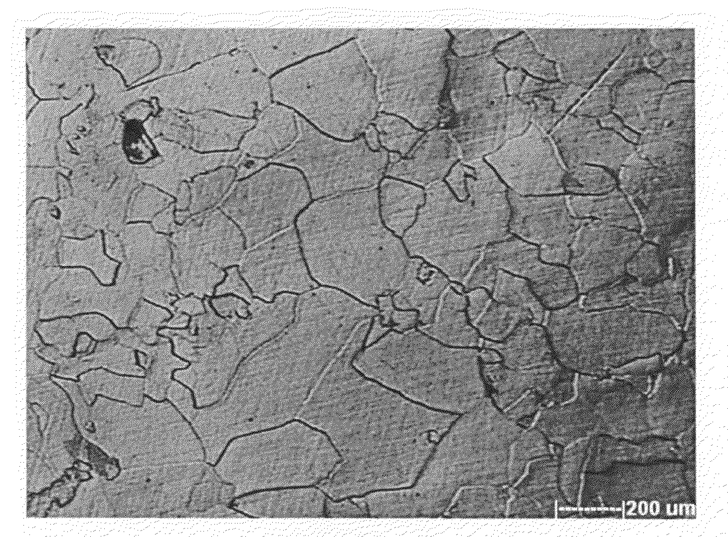
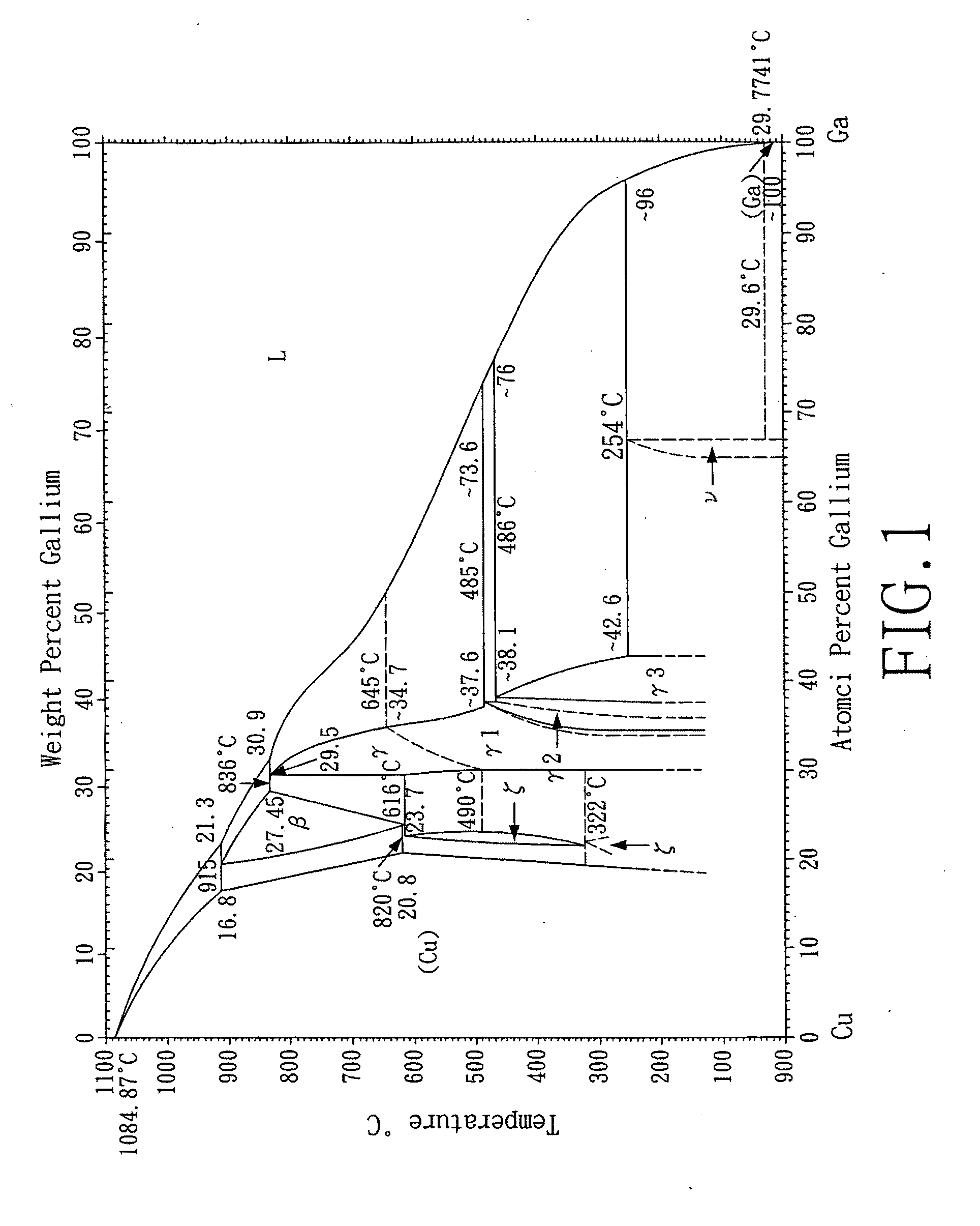
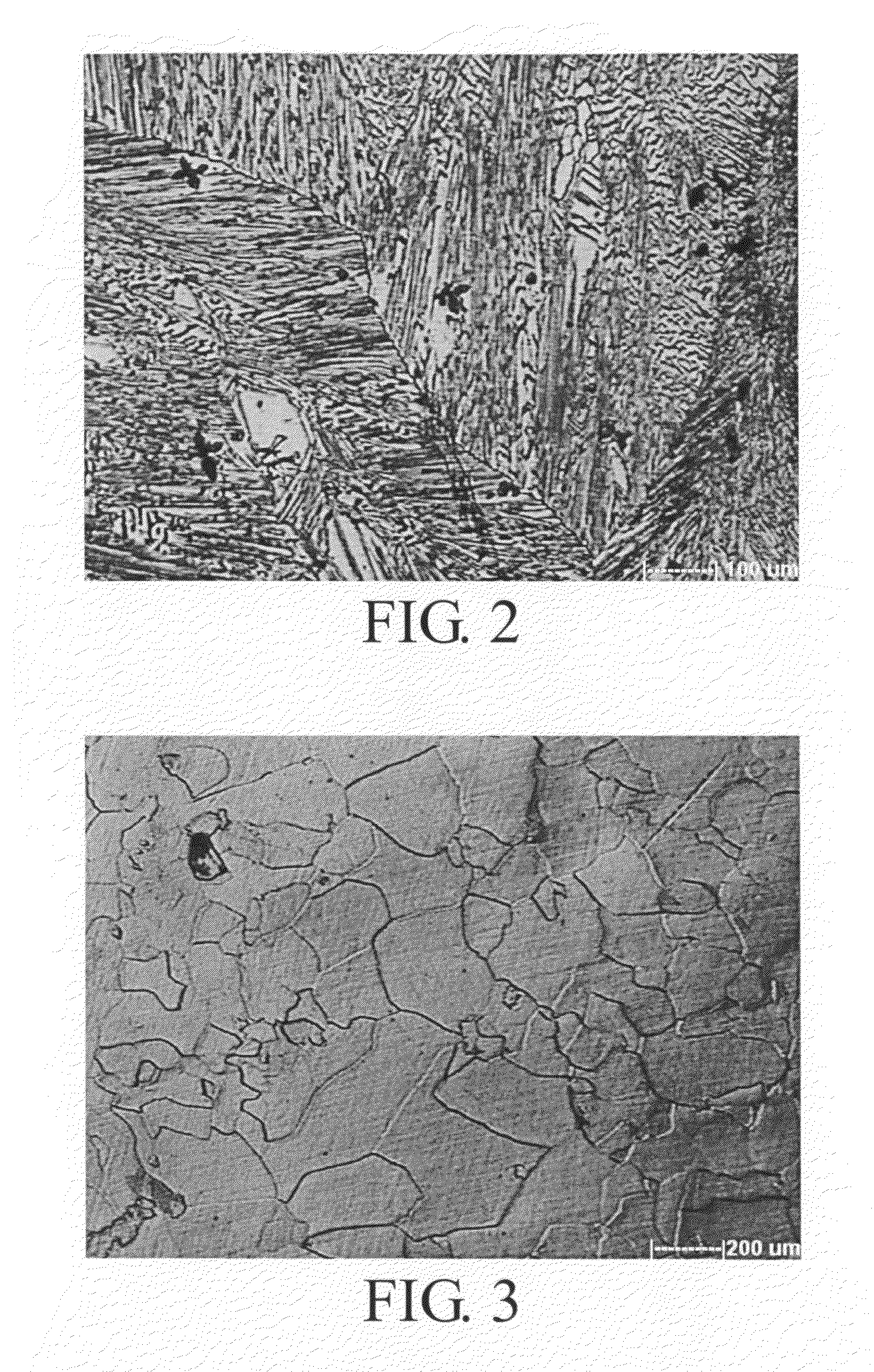
The present invention provides a method for making a copper-gallium alloy sputtering target that has a solid-solution phase and does not induce micro arcing during sputtering. This results in a consistent sputtering rate and a uniform copper-gallium thin film with improved quality and properties. The method involves treating the raw target with at least one thermal treatment between 500° C. and 850° C, followed by cooling to room temperature. The treated target has a compound phase not more than 25% on its metallurgical microstructure.

Problems solved by technology

When powder metallurgy is used, because gallium and indium both have low melting points, they are hard to be sintered.
Furthermore, a procedure for retrieving target residues is complicated, which increases cost of production of the sputter target.
(1) the copper target has non-uniform distribution of materials, resulting in macro segregation or micro segregation;
(2) two phases of the copper-alloy target result in a non-uniform thin film with poor properties (such as light-electricity conversion efficiency and the like);
(3) two phases of the Cu alloy target induce micro arcing during sputtering, which results in a thin film with poor quality.
Therefore, a cost of production and efficiency of the CIGS solar cell is dependent on the sputter target.

Method used


Image

  • Copper-gallium allay sputtering target, method for fabricating the same and related applications
  • Copper-gallium allay sputtering target, method for fabricating the same and related applications
  • Copper-gallium allay sputtering target, method for fabricating the same and related applications

Examples


example 1

[0050]A raw target was formed by vacuum melting. The raw target was treated by rolling at 800° C. at a reduction ratio of 25%, then was treated by thermal annealing treatment at 700° C. for 1 hour and cooled to room temperature to form a Cu—Ga alloy sputtering target.

example 2

[0051]A raw target was formed by air melting. The raw target was treated by thermal annealing treatment at 800° C. for 1 hour and then was treated by rolling at 800° C. at a reduction ratio of 25% then cooled to room temperature to form a Cu—Ga alloy sputtering target.

example 3

[0052]A raw target was formed by vacuum melting. The raw target was treated by hot-press sintering at 600° C. then was treated by thermal annealing treatment at 800° C. for 1 hour, before being cooled to room temperature to form a Cu—Ga alloy sputtering target.


PUM

PropertyMeasurementUnit
grain sizeaaaaaaaaaa
melting pointsaaaaaaaaaa
temperatureaaaaaaaaaa

Abstract

A method for fabricating a copper-gallium alloy sputtering target comprises forming a raw target; treating the raw target with at least one thermal treatment between 500° C.˜850° C. being mechanical treatment, thermal annealing treatment for 0.5˜5 hours or a combination thereof to form a treated target; and cooling the treated target to a room temperature to obtain the copper-gallium alloy sputtering target that has 71 atomic % to 78 atomic % of Cu and 22 atomic % to 29 atomic % of Ga and having a compound phase not more than 25% on its metallographic microstructure. Therefore, the copper-gallium alloy sputtering target does not induce micro arcing during sputtering so a sputtering rate is consistent and forms a uniform copper-gallium thin film. Accordingly, the copper-gallium thin film possesses improved quality and properties.

Description

BACKGROUND OF THE INVENTION[0001]1. Field of Invention[0002]The present invention relates to a method for fabricating a sputtering target, and more particularly to a method for fabricating a copper-gallium alloy sputtering target comprising a solid-solution phase principally.[0003]2. Description of the Related Art[0004]Non-renewable fuels are being exhausted, with peak oil, coal and gas approaching and nuclear requiring0 significant clean up costs, development of renewable energy is increasingly important. Photovoltaic solar cells, convert solar radiation directly into electricity for later use and include wafer type solar cells and thin-film type solar cells. Wafer type solar cells are current market leaders but have an indirect band gap for absorbing light, so a thick substrate layer of silicon (Si) is required. Since quantities of silicon are also limited, and the thick substrate raises production costs and practical usage, thin-film type solar cells are preferred in many instanc...

Claims


Application Information

Patent Timeline
Patent Type & Authority Applications(United States)
IPC IPC(8): C23C14/34C22F1/08B22F3/10B22D13/00C21D1/00B22F3/24C22C9/00H01L31/04
CPCB22F3/24B22F2003/248B22F2998/10C22C1/0425C22C9/00C22F1/08C23C14/3414H01L31/0264H01L31/04H01L31/18B22F3/15B22F3/17B22F3/12B22F3/18
Inventor HUANG, WEI-CHINTU, CHENG-HSIN
Owner SOLAR APPLIED MATERIALS TECHNOLOGY CORPORATION
Learn More