Field-effect transistor, and process for producing field-effect transistor

a field-effect transistor and field-effect technology, applied in transistors, electrical equipment, semiconductor devices, etc., can solve the problems of high energy cost, difficult film formation directly on a large-sized glass substrate, and inability to meet the requirements of high-efficiency semiconductor devices, so as to achieve the effect of reducing the degree of freedom of the production process and facilitating the production of semiconductor devices

Active Publication Date: 2010-05-13
IDEMITSU KOSAN CO LTD
View PDF4 Cites 53 Cited by
  • Summary
  • Abstract
  • Description
  • Claims
  • Application Information

AI Technical Summary

Benefits of technology

[0094]Due to the PAN resistance, the degree of freedom of the production proce

Problems solved by technology

A transistor using the above-mentioned silicon thin film is produced by using a silane-based gas, and hence, it is disadvantageous in respect of safety or equipment cost.
In addition, since an amorphous silicon thin film has a small band gap, it may absorb visible rays to ca

Method used


Image

  • Field-effect transistor, and process for producing field-effect transistor
  • Field-effect transistor, and process for producing field-effect transistor
  • Field-effect transistor, and process for producing field-effect transistor

Examples


first embodiment

[0104]FIG. 10 is a schematic flow chart for explaining the method for producing a field-effect thin film transistor according to the present invention;

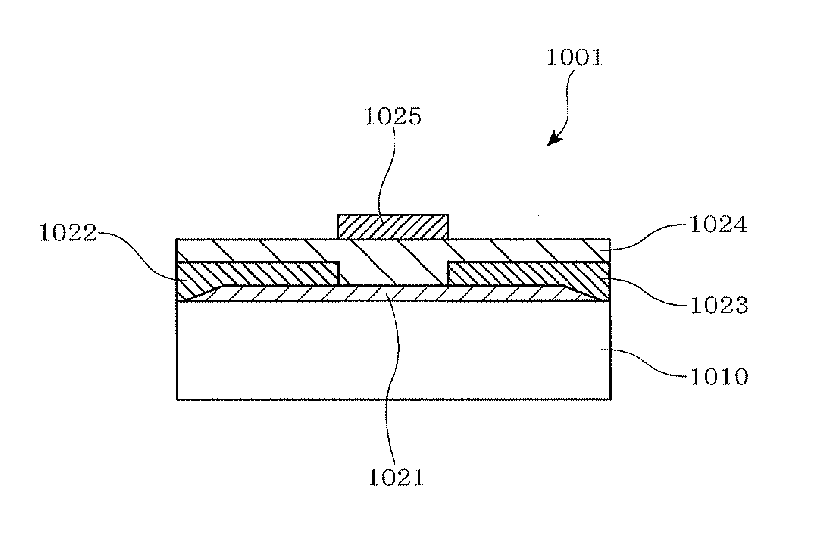
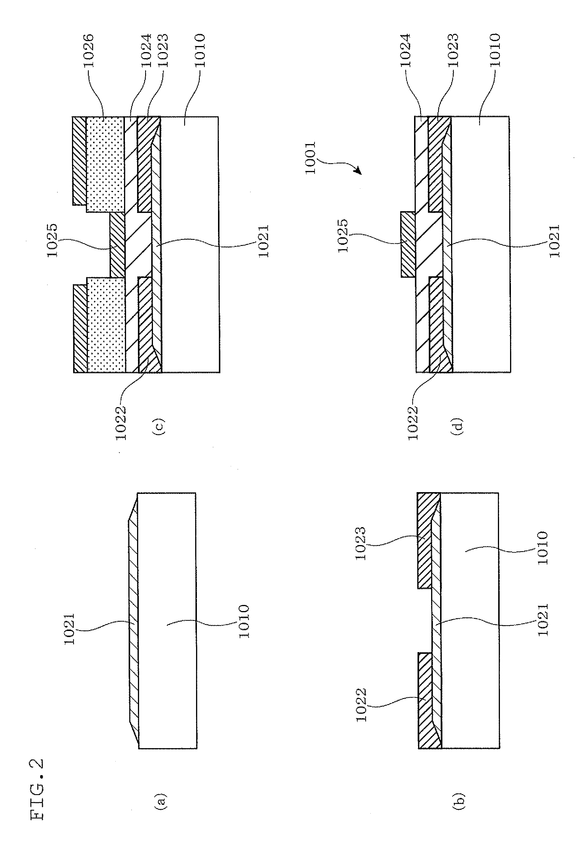
[0105]FIG. 11 is a schematic view of essential parts for explaining the method for producing a field-effect thin film transistor according to the first embodiment of the present invention, in which (a) is a cross-sectional view of a substrate which has been cleaned, (b) is a cross-sectional view showing the state in which an active layer is formed, (c) is a cross-sectional view showing the state in which a source electrode and a drain electrode are formed, (d) is a cross-sectional view showing the state in which a gate-insulating film is stacked, and (e) is a cross-sectional view showing the state in which the gate electrode is formed;

second embodiment

[0106]FIG. 12 is a schematic flow chart for explaining the method for producing a field-effect thin film transistor according to the present invention;

[0107]FIG. 13 is a schematic view of essential parts for explaining the method for producing a field-effect thin film transistor according to the second embodiment of the present invention, in which (a) is a cross-sectional view of a substrate which has been cleaned, (b) is a cross-sectional view showing the state in which an amorphous oxide to be served as an active layer is formed into a film, (c) is a cross-sectional view showing the state in which the crystalline oxide as the active layer is formed, (d) is a cross-sectional view showing the state in which a source electrode and a drain electrode are formed, (e) is a cross-sectional view showing the state in which a gate-insulating film is stacked and (f) is a cross-sectional view showing the state in which a gate electrode is formed;

third embodiment

[0108]FIG. 14 is a schematic flow chart for explaining the method for producing a field-effect thin film transistor according to the present invention;

[0109]FIG. 15 is a schematic view of essential parts for explaining the method for producing a field-effect thin film transistor according to the third embodiment of the present invention, in which (a) is a cross-sectional view of a substrate on which a gate electrode and a gate-insulating film are formed, (b) is a cross-sectional view showing the state in which an active layer and a conductor layer are formed into a film and a resist is formed by a half-tone mask, (c) is a cross-sectional view showing the state in which the active layer and the conductor layer are etched and the resist is re-formed, and (d) is a cross-sectional view showing the state in which a source electrode and a drain electrode are formed;

[0110]FIG. 16 is a schematic view of the sputtering apparatus by which the crystalline oxide according to Film-forming Exampl...


PUM


Abstract

To provide a field-effect transistor improved in transparency, electrical properties, stability, uniformity, reproducibility, heat resistance and durability, and as a reduced overlap capacity between electrodes.
A field-effect thin film transistor 1001 includes a gate electrode 1025, an active layer, a source electrode 1022 and a drain electrode 1023, wherein a crystalline oxide 1021 containing indium and having an electron carrier concentration of less than 1018/cm3 is used as the active layer, and the gate electrode 1025 is in self-alignment with the source electrode 1022 and the drain electrode 1023. The crystalline oxide 1021 contains a positive trivalent element different from a positive divalent element or indium.

Description

TECHNICAL FIELD[0001]The present invention relates to a field-effect transistor and a method for producing a field-effect transistor. In this field-effect transistor, a crystalline oxide with a predetermined electron carrier concentration is used as an active layer, and a gate electrode is in self-alignment with a source electrode and a drain electrode. In the method for producing a field-effect transistor, a crystalline oxide with a prescribed electron carrier concentration is used as an active layer.BACKGROUND ART[0002]An active-matrix type display apparatus such as an LCD (liquid crystal display) and an organic EL (Electro Luminescence) display apparatus is widely used in respect of display performance, energy saving, or the like. In particular, the active-matrix type display apparatus has almost come to constitute the mainstream of a display for cellular phones, PDAs (personal digital assistance), PCs, lap-top PCs, TVs or the like. In these display apparatuses, a TFT (field-effe...

Claims


Application Information

Patent Timeline
IPC IPC(8): H01L29/786H01L21/336
CPCH01L29/7869H01L29/66969
Inventor INOUE, KAZUYOSHIYANO, KOKIKASAMI, MASASHI
Owner IDEMITSU KOSAN CO LTD
Why Eureka
Try Eureka