Semiconductor device

a semiconductor device and semiconductor technology, applied in thermoelectric devices, instruments, non-linear optics, etc., can solve the problems of difficult to satisfactorily prevent moisture and oxygen from being mixed into the oxide semiconductor, easy cracking, and change of the semiconductor characteristics of the oxide semiconductor, so as to achieve the effect of improving the reliability of the semiconductor device, suppressing the variation of the semiconductor characteristics of the semiconductor device in which the oxide semiconductor is used, and high barrier property

Active Publication Date: 2010-05-13
SEMICON ENERGY LAB CO LTD
View PDF99 Cites 231 Cited by
  • Summary
  • Abstract
  • Description
  • Claims
  • Application Information

AI Technical Summary

Benefits of technology

[0018]According to an embodiment of the present invention, a film having a high barrier property against an impurity such as moisture and oxygen is used to prevent an impurity such as moisture and oxygen from being mixed into an oxide semiconductor, so that variation in semiconductor characteristics of a semiconductor device in which an oxide semiconductor is used can be suppressed. Further, reliability of the semiconductor device can be improved.

Problems solved by technology

However, by using a silicon oxide film or a silicon nitride film, it has been difficult to satisfactorily prevent moisture and oxygen from being mixed into the oxide semiconductor.
In addition, if the thickness of a silicon oxide film or a silicon nitride film is increased in order to prevent penetration of moisture and oxygen, a crack is easily caused.
Moreover, there is a problem in that semiconductor characteristics of an oxide semiconductor are changed when an impurity such as an alkali metal (Li, Cs, Na, or the like), an alkaline earth metal (Ca, Mg, or the like), or another metal element as well as moisture and oxygen are diffused into the oxide semiconductor.

Method used


Image

  • Semiconductor device
  • Semiconductor device
  • Semiconductor device

Examples


embodiment 1

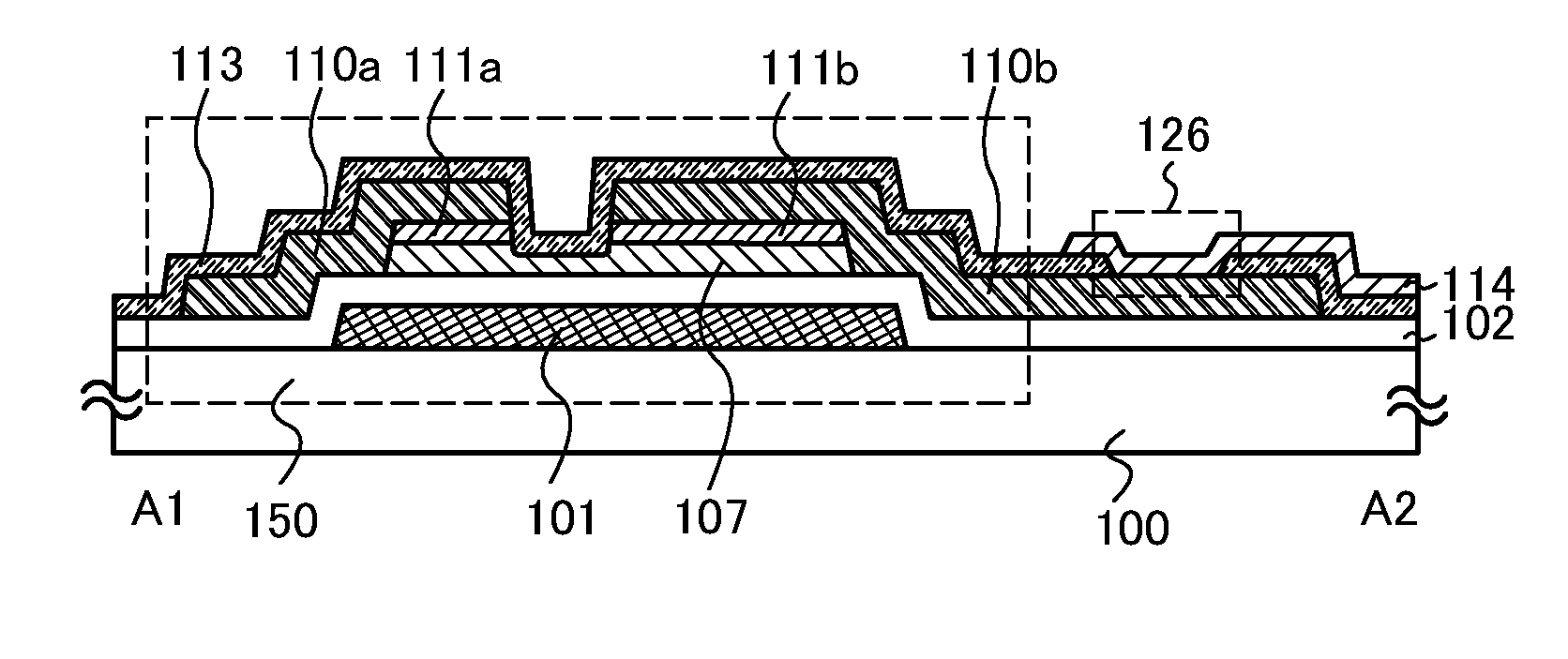
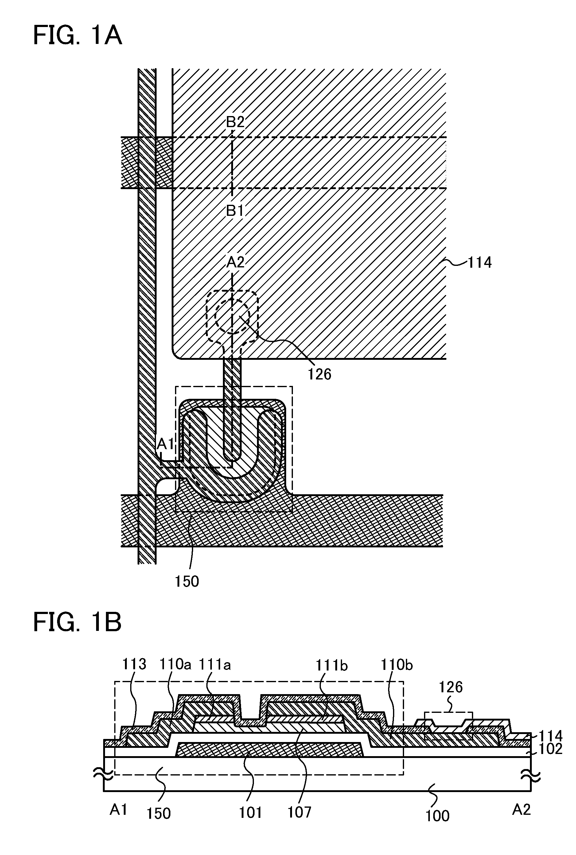
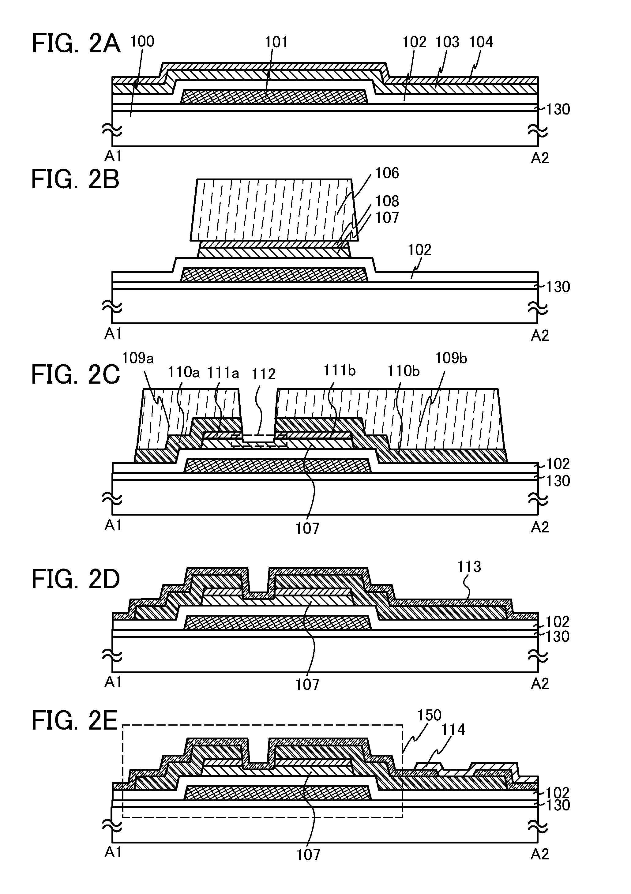
[0051]In this embodiment, semiconductor devices and manufacturing methods thereof are described with reference to FIGS. 1A and 1B, FIGS. 2A to 2E, FIGS. 3A to 3C, FIGS. 4A to 4C, FIGS. 5A1, 5A2, 5B1, and 5B2, and FIG. 6.

[0052]FIGS. 1A and 1B illustrate a pixel including a thin film transistor of this embodiment. FIG. 1A is a plan view and FIG. 1B is a cross-sectional view taken along line A1-A2 in FIG. 1A.

[0053]A thin film transistor 150 illustrated in FIGS. 1A and 1B is a so-called inverted-staggered thin film transistor. The thin film transistor 150 includes a gate electrode layer 101 provided over a substrate 100, a gate insulating film 102 covering the gate electrode layer 101, an oxide semiconductor layer 107 provided over the gate insulating film 102, a pair of oxide semiconductor layers 111a and 111b which are provided over and in contact with the oxide semiconductor layer 107 and are separated from each other, and a pair of conductive layers 110a and 110b which are in contac...

embodiment 2

[0135]In this embodiment, a semiconductor device which is different from that of Embodiment 1 and a manufacturing process thereof are described with reference to FIGS. 7A and 7B, FIGS. 8A to 8C, FIGS. 9A and 9B, and FIGS. 10A to 10C. Note that many portions of the semiconductor device and the manufacturing process described in this embodiment are same as those described in Embodiment 1. Therefore, description of the same portions is omitted and description of different portions is made below in detail.

[0136]FIGS. 7A and 7B illustrate a thin film transistor of this embodiment. FIG. 7A is a plan view, and FIG. 7B is a cross-sectional view taken along line A1-A2 of FIG. 7A.

[0137]FIGS. 7A and 7B illustrate a thin film transistor 250 in which a gate electrode layer 201 is formed over a substrate 200 having an insulating surface and a gate insulating film 202 is formed over the gate electrode layer 201. Conductive layers 210a and 210b functioning as a source electrode and a drain electrod...

embodiment 3

[0163]In this embodiment, a semiconductor device which is different from those of Embodiments 1 and 2 and a manufacturing process thereof are described with reference to FIGS. 11A and 11B and FIGS. 12A to 12D. Note that many portions of the manufacturing process described in this embodiment are same as those described in Embodiments 1 and 2. Therefore, description of the same portions is omitted and description of different portions is made in detail.

[0164]FIGS. 11A and 11B illustrate a thin film transistor of this embodiment. FIG. 11A is a plan view and FIG. 11B is a cross-sectional view taken along line A1-A2 of FIG. 11A.

[0165]FIGS. 11A and 11B illustrate a thin film transistor 350 in which a gate electrode layer 301 is formed over a substrate 300 having an insulating surface, and a gate insulating film 302 is formed over the gate electrode layer 301. An oxide semiconductor layer 307 and a channel protective layer 315 which covers a region overlapping with a channel formation regi...


PUM


Abstract

An object is to prevent an impurity such as moisture and oxygen from being mixed into an oxide semiconductor and suppress variation in semiconductor characteristics of a semiconductor device in which an oxide semiconductor is used. Another object is to provide a semiconductor device with high reliability. A gate insulating film provided over a substrate having an insulating surface, a source and a drain electrode which are provided over the gate insulating film, a first oxide semiconductor layer provided over the source electrode and the drain electrode, and a source and a drain region which are provided between the source electrode and the drain electrode and the first oxide semiconductor layer are provided. A barrier film is provided in contact with the first oxide semiconductor layer.

Description

TECHNICAL FIELD[0001]The present invention relates to a semiconductor device in which an oxide semiconductor is used and a manufacturing method thereof.BACKGROUND ART[0002]As typically seen in a liquid crystal display device, a thin film transistor formed over a flat plate such as a glass substrate is manufactured using amorphous silicon or polycrystalline silicon. A thin film transistor manufactured using amorphous silicon has low field effect mobility, but can be formed over a larger glass substrate. In contrast, a thin film transistor manufactured using crystalline silicon has high field effect mobility, but due to a crystallization step such as laser annealing, such a transistor is not always suitable for being formed over a larger glass substrate.[0003]Techniques have attracted attention, in which a thin film transistor using an oxide semiconductor is manufactured and applied to electronic devices or optical devices. For example, Patent Document 1 and Patent Document 2 disclose...

Claims


Application Information

Patent Timeline
Patent Type & Authority Applications(United States)
IPC IPC(8): H01L29/26
CPCH01L27/1225H01L29/66742H01L29/66969H01L29/7869H01L29/78606G02F1/1368H01L29/41733H01L29/78618H01L27/1248
Inventor AKIMOTO, KENGOYAMAZAKI, SHUNPEI
Owner SEMICON ENERGY LAB CO LTD
Why Eureka
Try Eureka