Semiconductor device and manufacturing method thereof

a semiconductor layer and semiconductor technology, applied in the field of semiconductor devices, can solve the problems that the transistor is not always suitable for being formed over a larger glass substrate, and achieve the effect of suppressing the degradation of the switching characteristics of the thin film transistor and improving the coverage of the oxide semiconductor layer provided over the source and drain electrodes

Active Publication Date: 2010-05-13
SEMICON ENERGY LAB CO LTD
View PDF100 Cites 40 Cited by
  • Summary
  • Abstract
  • Description
  • Claims
  • Application Information

AI Technical Summary

Benefits of technology

[0041]The angle formed by the surface of the substrate and the side surface of the source electrode and the angle formed by the surface of the substrate and the side surface of the drain electrode are adjusted, so that the coverage by the oxide semiconductor layer provided over the source and drain electrodes is improved.
[0042]An electric-field relaxation region is provided, so that electric-field concentration which might occur between the source and drain electrodes is relaxed and degradation of the switching characteristics of the thin film transistor is suppressed.

Problems solved by technology

In contrast, a thin film transistor manufactured using crystalline silicon has high field effect mobility, but due to the necessity of a crystallization step such as laser annealing, such a transistor is not always suitable for being formed over a larger glass substrate.

Method used


Image

  • Semiconductor device and manufacturing method thereof
  • Semiconductor device and manufacturing method thereof
  • Semiconductor device and manufacturing method thereof

Examples


embodiment 1

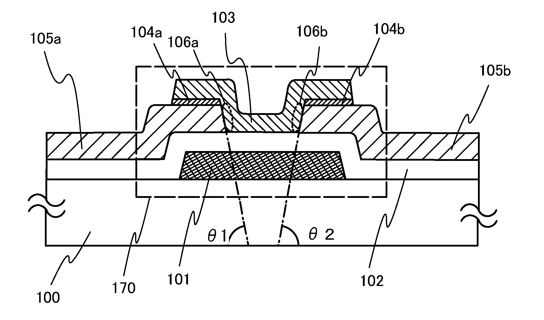
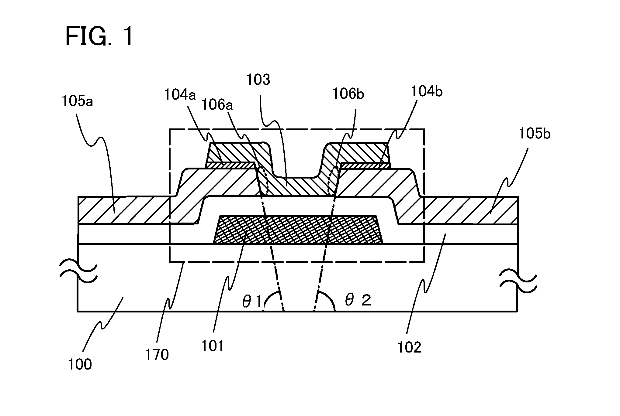
[0081]The case in which a thin film transistor 170 is provided over a substrate is illustrated in FIG. 1. FIG. 1 is one example of a cross-sectional view of a thin film transistor.

[0082]A gate electrode 101 provided over a substrate 100 having an insulating surface is covered with a gate insulating layer 102, and a first wiring and a second wiring are provided over the gate insulating layer 102 which overlaps with the gate electrode 101. A buffer layer is provided over each of the first wiring and the second wiring which function as a source electrode layer 105a and a drain electrode layer 105b. A first buffer layer 104a is provided over the source electrode layer 105a, and a second buffer layer 104b is provided over the drain electrode layer 105b. An oxide semiconductor layer 103 is provided over the first buffer layer 104a and the second buffer layer 104b.

[0083]In FIG. 1, as the substrate 100 having a light-transmitting property, a glass substrate of barium borosilicate glass, al...

embodiment 2

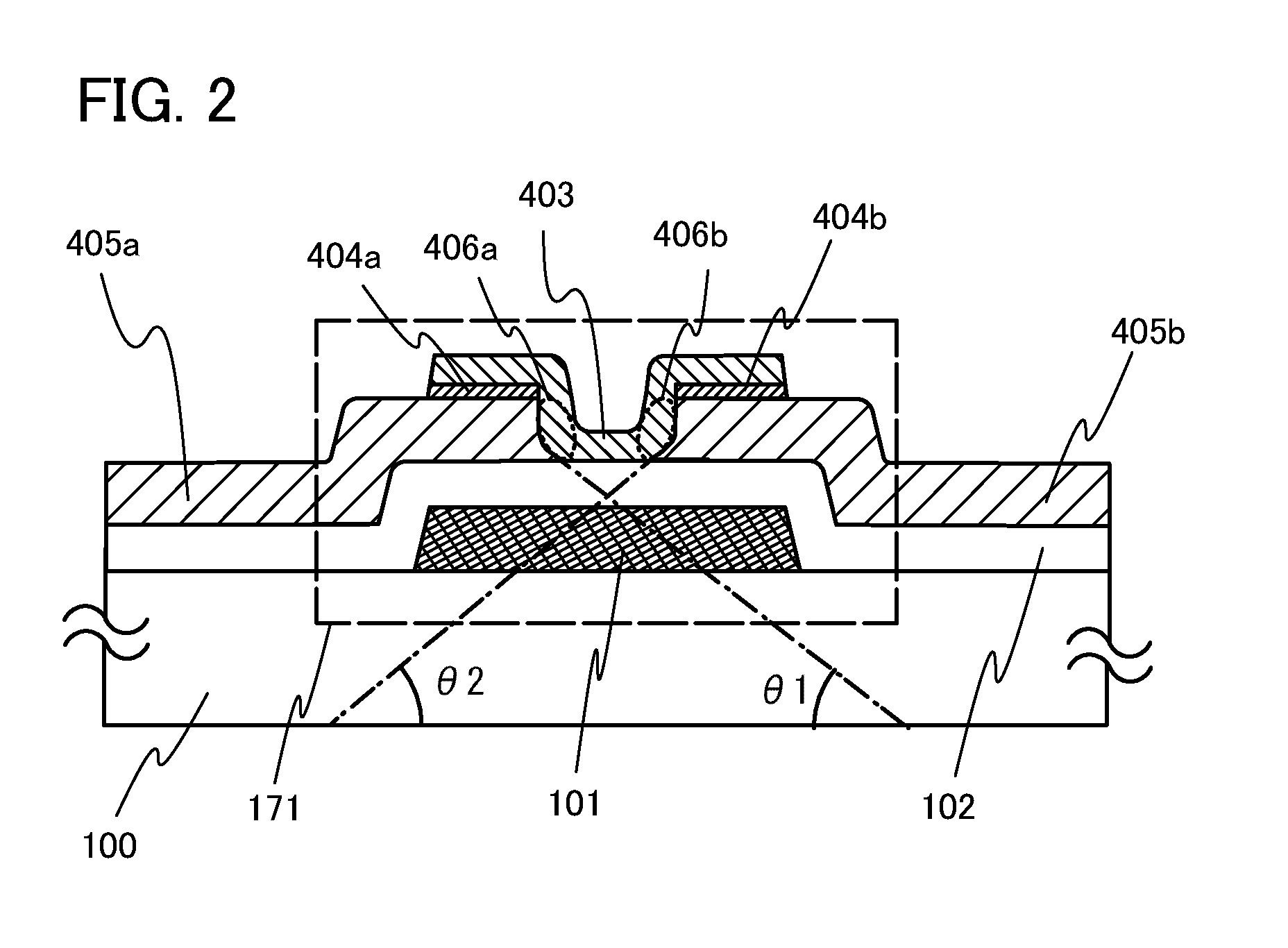
[0096]The case where the straight line which connects the top edge of the side surface of the source electrode layer (or the drain electrode layer) to the bottom edge of the side surface of the source electrode layer (or the drain electrode layer) substantially coincides with the slope of the side surface of the source electrode layer (or the drain electrode layer) is illustrated in FIG. 1. In Embodiment 2, the case where the side surface of a source electrode layer (or a drain electrode layer) has a step will be described using FIG. 2. The side surface of the electrode may have a step as long as angle θ1 of the side surface of the bottom edge of the source electrode layer and angle θ2 of the side surface of the bottom edge of the drain electrode layer each are greater than or equal to 20° and less than 90°. Note that, in FIG. 2, the same reference numerals are used for the portions that are common to those in FIG. 1.

[0097]A gate electrode 101 provided over a substrate 100 having an...

embodiment 3

[0109]In this embodiment, a thin film transistor and a manufacturing process thereof are described with reference to FIGS. 3A and 3B, 4A to 4C, 5 to 8, and FIGS. 9A1 and 9A2 and 9B1 and 9B2.

[0110]In FIG. 3A, as a substrate 100 having a light-transmitting property, a glass substrate of barium borosilicate glass, aluminoborosilicate glass, or the like can be used.

[0111]Then, a conductive layer is formed over the entire surface of the substrate 100, a first photolithography step is performed to form a resist mask, and an unnecessary portion is removed by etching to form wirings and an electrode (a gate wiring including a gate electrode 101, a capacitor wiring 108, and a first terminal 121). At this time, the etching is performed so that at least the edge portion of the gate electrode 101 is tapered. FIG. 3A is a cross-sectional view at this stage. A top view at this stage corresponds to FIG. 5.

[0112]The gate wiring including the gate electrode 101, the capacitor wiring 108, and the fir...


PUM


Abstract

A structure by which electric-field concentration which might occur between a source electrode and a drain electrode in a bottom-gate thin film transistor is relaxed and deterioration of the switching characteristics is suppressed, and a manufacturing method thereof. A bottom-gate thin film transistor in which an oxide semiconductor layer is provided over a source and drain electrodes is manufactured, and angle θ1 of the side surface of the source electrode which is in contact with the oxide semiconductor layer and angle θ2 of the side surface of the drain electrode which is in contact with the oxide semiconductor layer are each set to be greater than or equal to 20° and less than 90°, so that the distance from the top edge to the bottom edge in the side surface of each electrode is increased.

Description

BACKGROUND OF THE INVENTION[0001]1. Field of the Invention[0002]The present invention relates to a display device using an oxide semiconductor and a method for manufacturing the same.[0003]2. Description of the Related Art[0004]As typically seen in liquid crystal display devices, a thin film transistor formed over a flat plate such as a glass substrate is manufactured using amorphous silicon or polycrystalline silicon. A thin film transistor manufactured using amorphous silicon has low field effect mobility, but can be formed over a larger glass substrate. In contrast, a thin film transistor manufactured using crystalline silicon has high field effect mobility, but due to the necessity of a crystallization step such as laser annealing, such a transistor is not always suitable for being formed over a larger glass substrate.[0005]In view of the foregoing, attention has been drawn to a technique in which a thin film transistor is manufactured using an oxide semiconductor and applied to...

Claims


Application Information

Patent Timeline
Patent Type & Authority Applications(United States)
IPC IPC(8): H01L29/786H01L21/34
CPCH01L21/02554H01L21/02565H01L21/02631H01L27/1225H01L29/41733H01L29/78696H01L29/786H01L27/1288H01L29/7869G02F1/1368G02F1/136213H10K59/1216H10K59/124H10K59/1213H01L29/4908H01L29/78618H10K10/46H10K10/84H10K10/462H10K10/466
Inventor YAMAZAKI, SHUNPEIAKIMOTO, KENGOKAWAE, DAISUKE
Owner SEMICON ENERGY LAB CO LTD
Why Eureka
Try Eureka