Power semiconductor device

a technology of power semiconductor and semiconductor device, which is applied in the direction of semiconductor device, semiconductor/solid-state device details, electrical apparatus, etc., can solve the problems of low productivity and prolonged manufacturing time, and achieve the effect of power semiconductor device, reduced size of present invention, and increased mounting density

Active Publication Date: 2010-05-13
MITSUBISHI ELECTRIC CORP
View PDF11 Cites 55 Cited by
  • Summary
  • Abstract
  • Description
  • Claims
  • Application Information

AI Technical Summary

Benefits of technology

[0015]The power semiconductor device according to the present invention has a structure in which the cylindrical external terminal communication section, to which the external terminal can be inserted and connected, is provided so as to be substantially perpendicular to the wiring pattern surface of the circuit substrate, and the top portion of the cylindrical external terminal communication section is exposed from the transfer molding resin. Accordingly, the external terminal can be inserted and connected to the cylindrical external terminal communication section, and the external terminal can be formed within a projection area of amounting surface for the power semiconductor device. Therefore, the power semiconductor device of the present invention can be reduced in size, and a space on an external circuit substrate or the like, which is necessary to mount the power semiconductor device, can be reduced.
[0016]In the case where multiple power semiconductor devices of the present invention are mounted on an external circuit substrate, even if adjacent power semiconductor devices are in close proximity to each

Problems solved by technology

Thus, there are a large number of manufacturing processes, causing a prolon

Method used


Image

  • Power semiconductor device
  • Power semiconductor device
  • Power semiconductor device

Examples


first embodiment

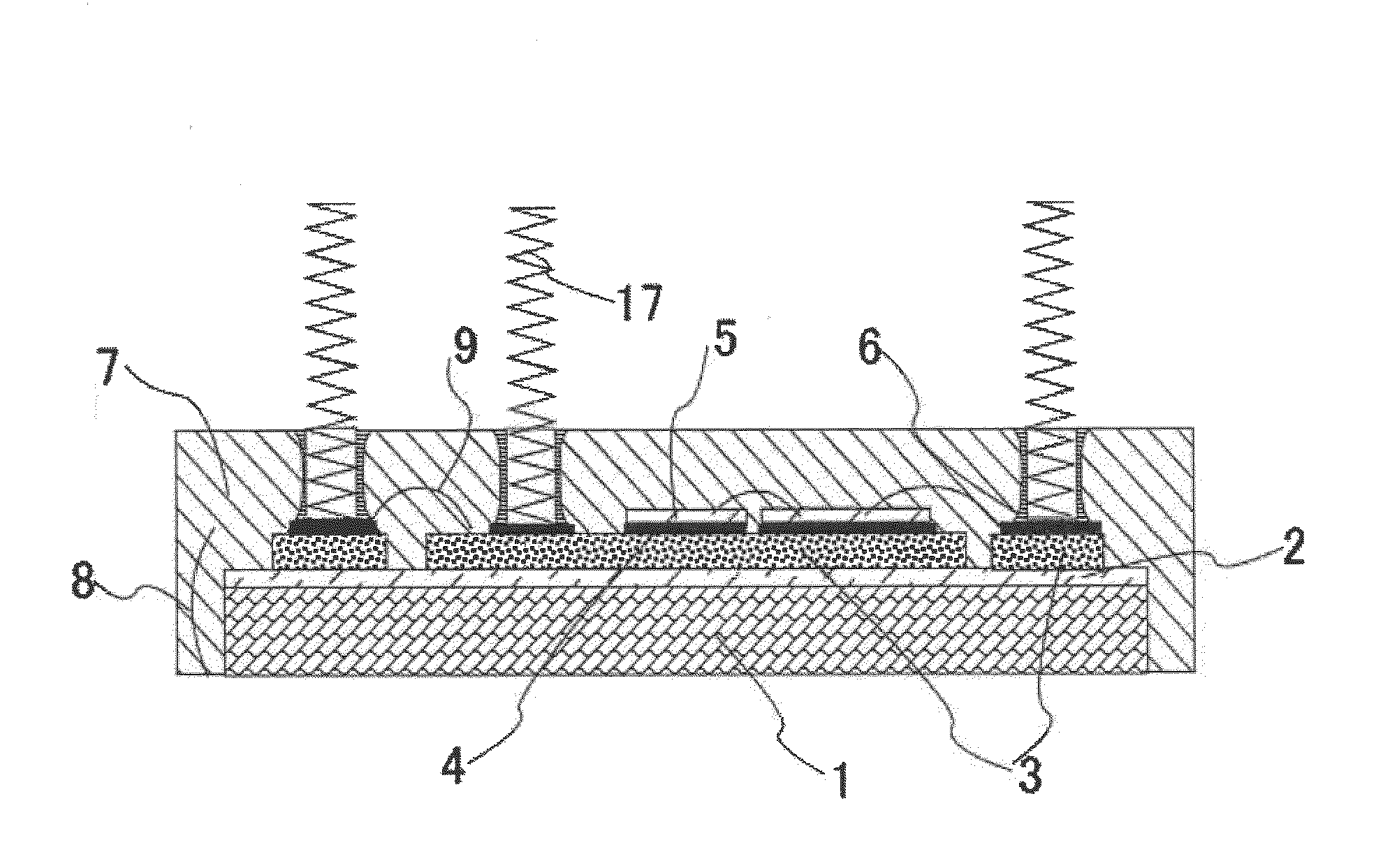
[0027]FIG. 1 is a schematic cross-sectional view showing a power semiconductor device according to the first embodiment of the present invention.

[0028]As shown in FIG. 1, in a power semiconductor device 100 of the present embodiment, a resin insulation layer 2, which is a high thermal conductive insulation layer, is provided on one surface of a metal plate 1 that acts as a metal heat dissipater for dissipating heat of the power semiconductor device 100. A surface of the resin insulation layer 2 has a metallic foil wiring pattern 3 provided thereon, which surface is opposite to a surface, of the resin insulation layer 2, joined to the metal plate 1.

[0029]That is, the metal plate 1, the resin insulation layer 2 and the wiring pattern 3 constitute a metallic circuit substrate 8 that is a circuit substrate. Power semiconductor elements 5 and cylindrical external terminal communication sections 6 are joined, by solder 4, to the wiring pattern 3 in a substantially perpendicular manner. Ne...

second embodiment

[0062]FIG. 3 is a schematic cross-sectional view showing a power semiconductor device according to the second embodiment of the present invention.

[0063]As shown in FIG. 3, a power semiconductor device 200 of the present embodiment is the same as the power semiconductor device according to the first embodiment except that rod-like external terminals 13 are inserted to the cylindrical external terminal communication sections 6 and that the external terminals 13 are electrically connected to a wiring circuit of the power semiconductor device.

[0064]In the present embodiment, a metal having excellent thermal conductivity and electrical conductivity is used for the external terminals 13. In particular, a copper material is preferred. Outer diameters of the external terminals 13 are properly determined based on the current carrying capacity of each power semiconductor element 5. The external terminals 13 each having a large outer diameter are used for the power semiconductor device 200 hav...

third embodiment

[0068]FIG. 4 is a schematic cross-sectional view showing a power semiconductor device according to the third embodiment of the present invention.

[0069]As shown in FIG. 4, a power semiconductor device 300 of the present embodiment is the same as the power semiconductor device of the second embodiment except that a ceramic circuit substrate 14 is used instead of the metallic circuit substrate 8.

[0070]As for the ceramic circuit substrate 14 of the present embodiment, a copper foil is joined to both surfaces of a ceramic plate 15 that is a high thermal conductive insulation layer. Similarly to the first embodiment, etching is performed on the copper foil provided on one of the surfaces of the ceramic plate 15, in order to form the wiring pattern 3, and the copper foil provided on the other surface, which is a copper foil 16, acts as a metal heat dissipater of the power semiconductor device 300.

[0071]In the present embodiment, alumina, aluminum nitride, silicon nitride, or the like is us...


PUM


Abstract

A power semiconductor device in which transfer molding resin seals: a metallic circuit substrate; a power semiconductor element joined to a wiring pattern; and a side surface of a cylindrical external terminal communication section provided on the wiring pattern and to which an external terminal can be inserted and connected. The cylindrical external terminal communication section is substantially perpendicular to a surface on which the wiring pattern is formed. An outer surface of a metal plate of the metallic circuit substrate and a top portion of the cylindrical external terminal communication section are exposed from the transfer molding resin. The transfer molding resin is not present within the cylindrical external terminal communication section.

Description

TECHNICAL FIELD[0001]The present invention relates to a resin-sealed power semiconductor device formed by transfer molding, which is excellent in productivity. The present invention particularly relates to a resin-sealed power semiconductor device formed by transfer molding, which is small in size and which realizes large-current operation.BACKGROUND ART[0002]A power semiconductor device, such as a power module, operates with a large current and a high voltage. For this reason, it is essential to efficiently discharge heat, which is generated by the operation of the power semiconductor device, to the outside of the power semiconductor device. Accordingly, in a power semiconductor device, a wiring pattern is formed on a metal plate that acts as a heat sink, while an insulation layer is interposed between the wiring pattern and the metal plate. A power semiconductor element is provided on the wiring pattern. The power semiconductor element is sealed with resin.[0003]One of such power ...

Claims


Application Information

Patent Timeline
IPC IPC(8): H01L23/48
CPCH01L23/4334H01L23/49811H01L2224/48227H01L2224/48137H01L2224/45124H01L2224/32225H01L24/48H01L2924/19107H01L2924/1532H01L2924/15312H01L2924/01078H01L2924/01004H01L2224/73265H01L2224/48091H01L25/072H01L2224/16H01L2924/00014H01L2924/00H01L2924/00012H01L2224/45015H01L24/45H01L24/73H01L2924/181
Inventor OKA, SEIJIUSUI, OSAMUNAKAYAMA, YASUSHIOBIRAKI, YOSHIKOOI, TAKESHI
Owner MITSUBISHI ELECTRIC CORP
Why Eureka
Try Eureka