

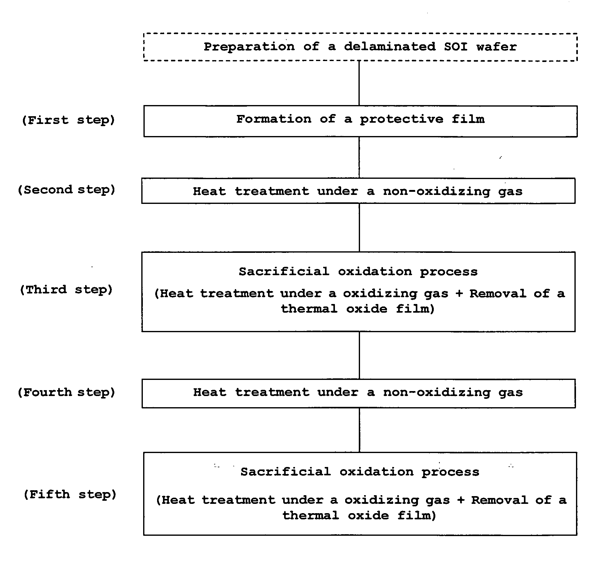
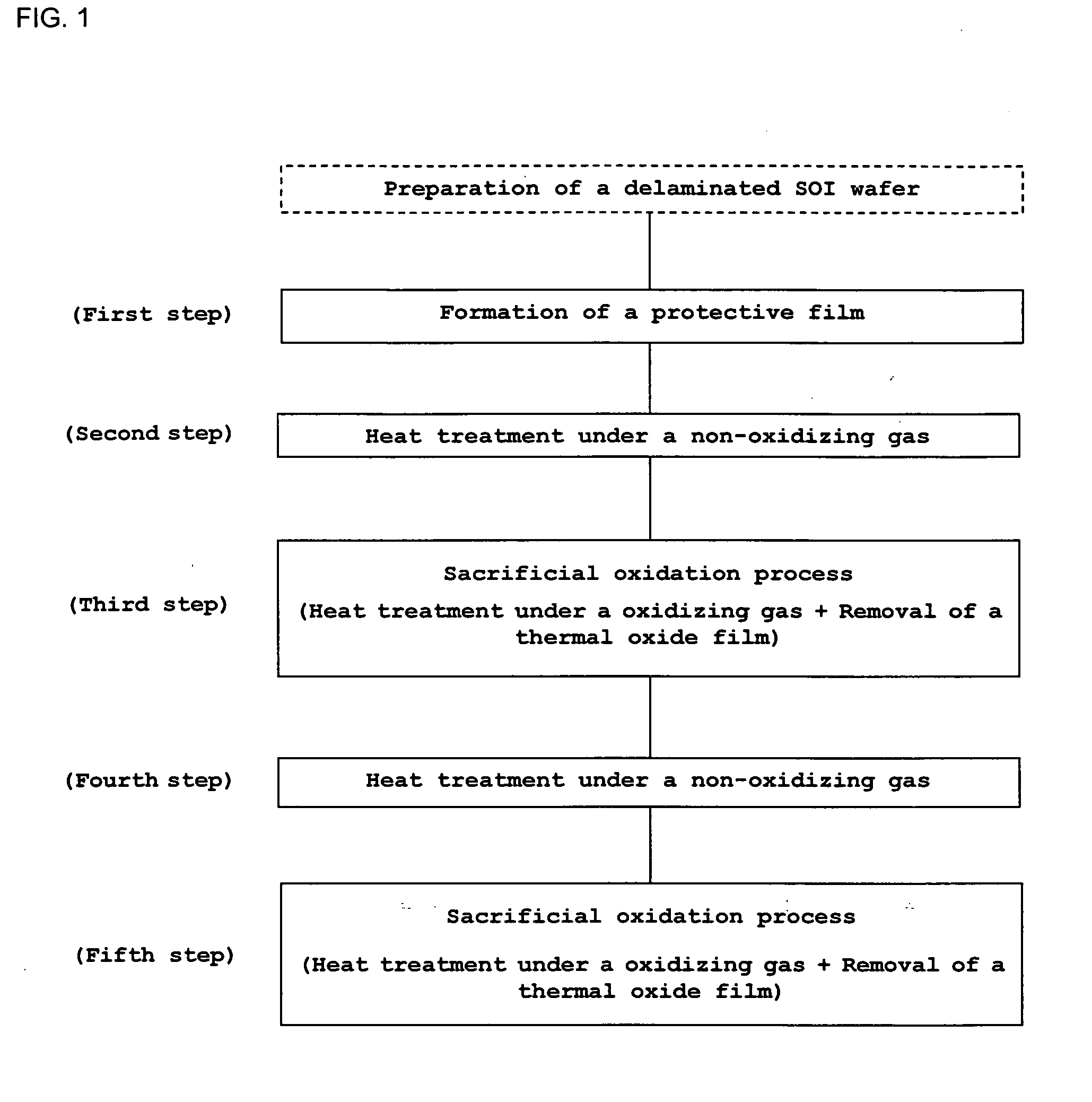
Method for manufacturing bonded wafer
a technology of bonded wafers and bonded layers, which is applied in the manufacturing of semiconductor/solid-state devices, electrical equipment, basic electric elements, etc., can solve the problems of remaining damage and affecting device characteristics, and achieve the effect of reducing the occurrence of concave defects, reducing surface roughness, and easy adjustmen
- Summary
- Abstract
- Description
- Claims
- Application Information
AI Technical Summary
Benefits of technology
Problems solved by technology
Method used
Image

Examples
example 1
[0069]An SOI wafer was fabricated by using the method for manufacturing a bonded wafer of the present invention.
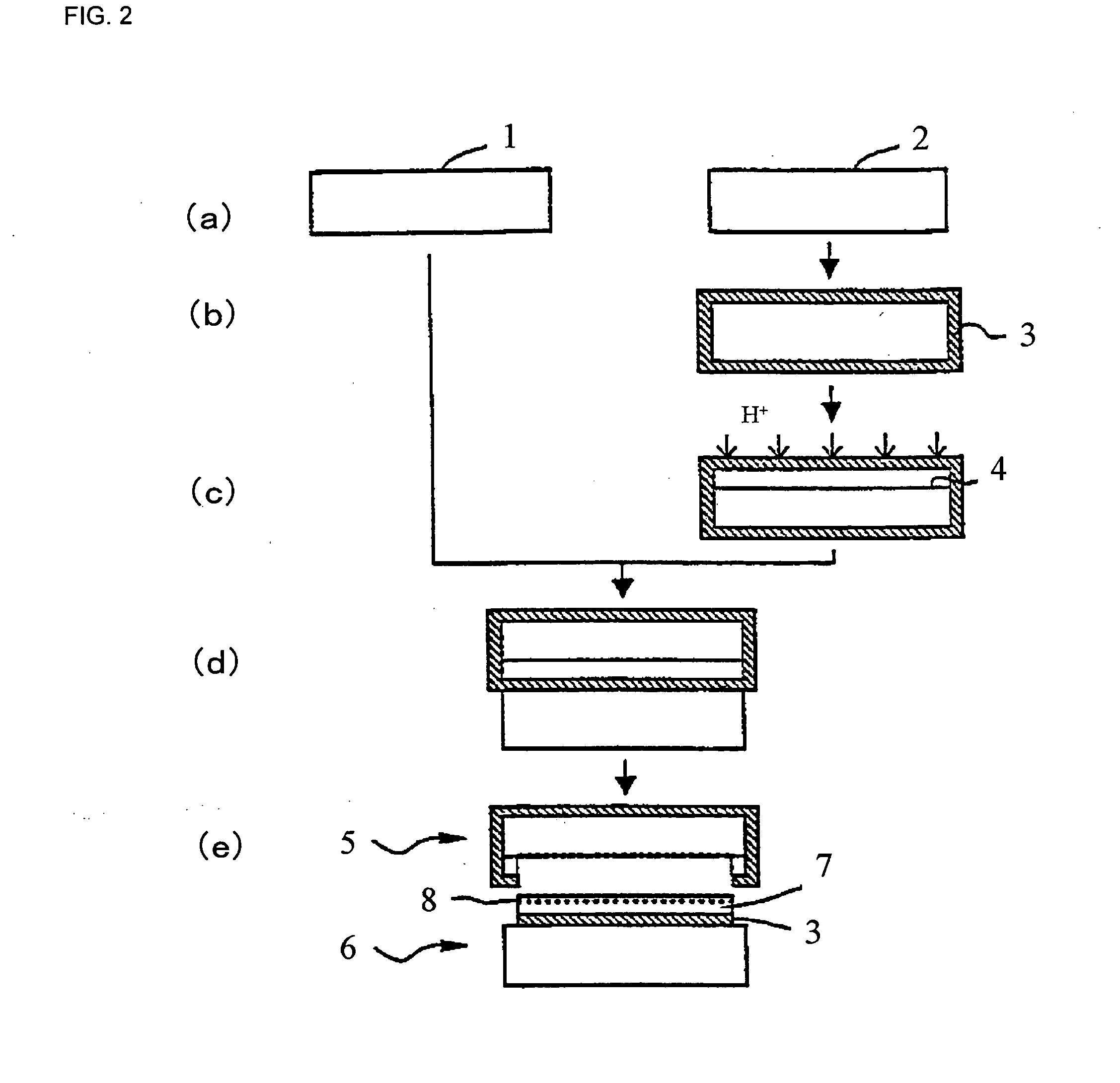
[0070]A silicon single crystal ingot produced by the Czochralski method and having a crystal orientation of , conductivity type of p-type and a resistivity of 10Ω·cm was sliced and processed to fabricate silicon mirror surface wafers having a diameter of 300 mm. These were divided into bond wafer and base wafer, and a SOI wafer having a thin film SOI layer on a surface was obtained as a sample by the process shown in FIG. 2.
[0071]It is to be noted that a thickness of the SOI layer was 400 nm and a thickness of a buried oxide film was 150 nm. Ion implanting conditions were that implanted ions were H+ ions, implantation energy was 50 keV and dose amount was 5.0×10¹⁶ / cm2. Moreover, delaminating heat treatment was heat treatment at 500° C. for 2 hours under N2 gas atmosphere.
[0072]The SOI wafer. after delaminating obtained as describe above was cleaned for 3 minutes using ozon...
example 2 , 3
EXAMPLE 2, 3
[0085]A SOI wafer was manufactured in the same conditions as Example 1 except that RTO process for forming an oxide film having a thickness of 3 nm (Example 2) and 4 nm (Example 3) on a SOI layer surface was performed in between the first step and the second step and the same evaluation as Example 1 carried out.
[0086]As a result, it is revealed that a thickness of the oxide film formed after the first step of the SOI wafer of Example 2 was 3.0 nm, pit density of the oxide film surface after the second step was 3×10⁸ numbers / cm2, and the oxide film surface was nonuniform. Moreover, the P-V value of the wafer surface after the fifth step was 2.3 nm and the concave defect density was 3×10² numbers / cm2. From the results, it was revealed that the SOI wafer surface of Example 2 was as flat as one of Example 1 and had few concave defects.
[0087]Moreover, it is revealed that a thickness of the oxide film formed after the first step of the SOI wafer of Example 3 was 4.0 nm, pit de...
PUM
 Abstract
Description
Claims
Application Information