Automated chemical polishing system adapted for soft semiconductor materials

a technology of automatic polishing and semiconductor materials, applied in the direction of grinding machine components, manufacturing tools, lapping machines, etc., can solve the problems of inability to withstand excessive downward pressure of the sort exerted in conventional polishing processes, less precision, and more fragile semiconductor materials, etc., to achieve smooth variation of downward pressure and enhanced precision

Active Publication Date: 2010-05-13
DRS NETWORK & IMAGING SYST
View PDF9 Cites 7 Cited by
  • Summary
  • Abstract
  • Description
  • Claims
  • Application Information

AI Technical Summary

Benefits of technology

[0005]The present invention is directed to resolving these problems of precision and control throughout the duration of the polishing operation, using components able to withstand harsh environmental conditions. According to one aspect of the invention, a polishing platen, which preferably rotates about its axis, is supported by a base. At least one workpiece (such as a wafer) is suspended above this platen by a mount on a jig shaft, which in turn is supported by a jig. Preferably, each component exposed to this work area is encapsulated in a chemically resistant material, such as polytetrafluoroethylene or polypropylene. As the workpiece is lowered onto the platen, a sensor, such as a load cell, senses that amount of a first weight, which includes the weight of the jig shaft, mount and workpiece, which continues to be supported by the jig. As the amount of the first weight supported by the jig decreases, the amount of the first weight which is supported by the platen increases, and therefore the pressure between the workpiece and the platen increases. Means such as a programmed controller may receive a signal from the load cell and control the up-and-down displacement of the jig shaft as a function of this signal. This feedback loop can regulate the amount of pressure between the platen and the workpiece.
[0006]It is preferred that the jig shaft be supported by the jig by means of a spring, and even more preferably by means of a helical compression spring. This spring allows a smooth variation in the amount of supported weight and more precise control, over a lengthened vertical displacement of the jig shaft.
[0011]The present invention thus provides polishing apparatus in which the motions of the platen and workpiece, and the pressure between them, are precisely controlled. The periodic measurement of the supported weight (and the comparison of that weight (or a calculated derivative of it) against a stored reference) allows continuous adjustment of downward pressure as the polishing operation progresses. The use of a spring to more smoothly vary the amount of downward pressure relative to vertical displacement of the jig shaft permits enhanced precision.

Problems solved by technology

Some semiconductor materials, particularly Group II-VI semiconductor materials and more particularly mercury cadmium telluride (MCT) and cadmium telluride (CT) materials, are more fragile and cannot withstand excessive downward pressure of the sort exerted in conventional polishing processes.
To date, conventional CP apparatus have been less than satisfactory in using only light pressures yet exerting sufficient control.
Several conventional semiconductor polishing systems do not provide for the use of chemical polishing solutions.

Method used


Image

  • Automated chemical polishing system adapted for soft semiconductor materials
  • Automated chemical polishing system adapted for soft semiconductor materials
  • Automated chemical polishing system adapted for soft semiconductor materials

Examples


Embodiment Construction

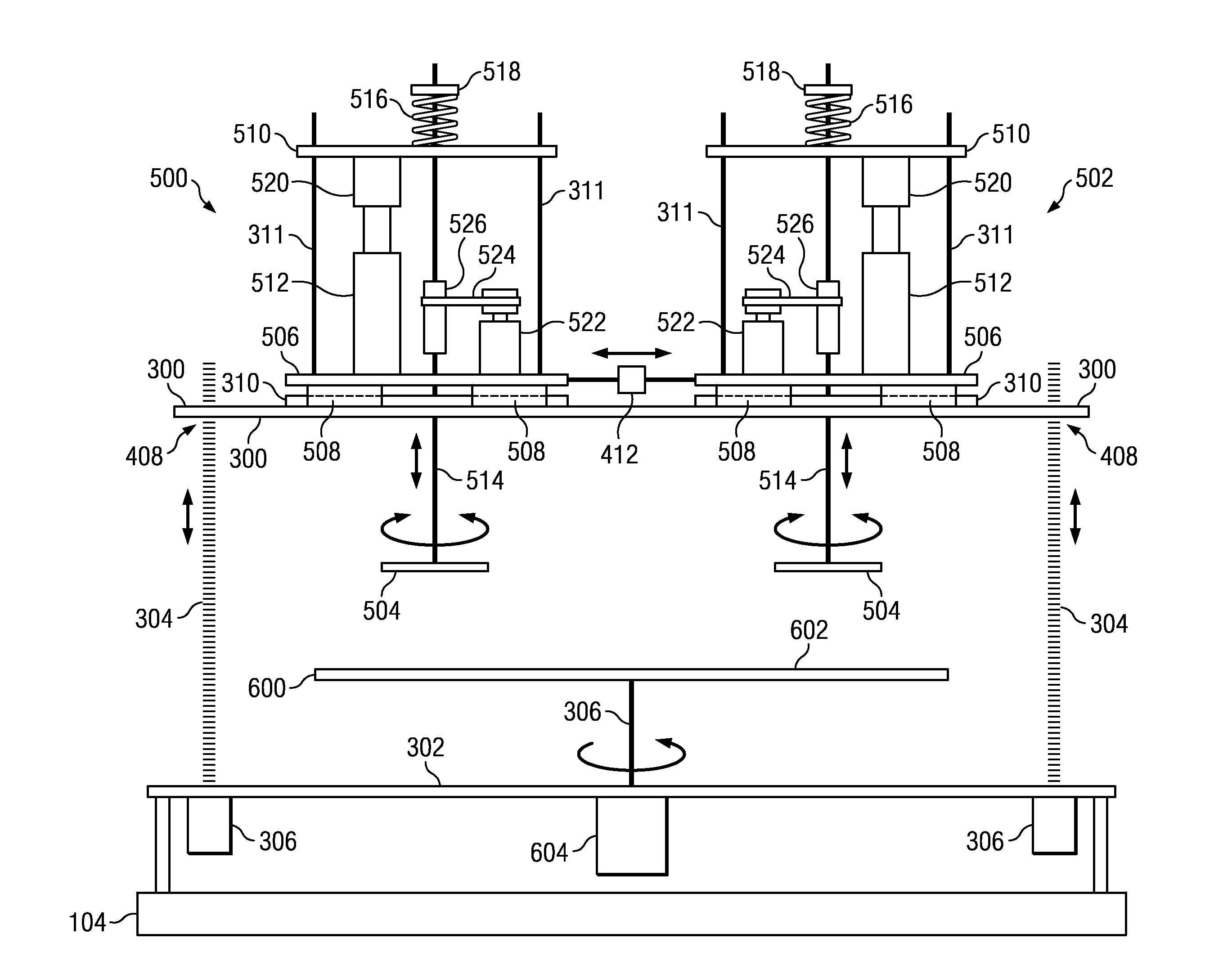
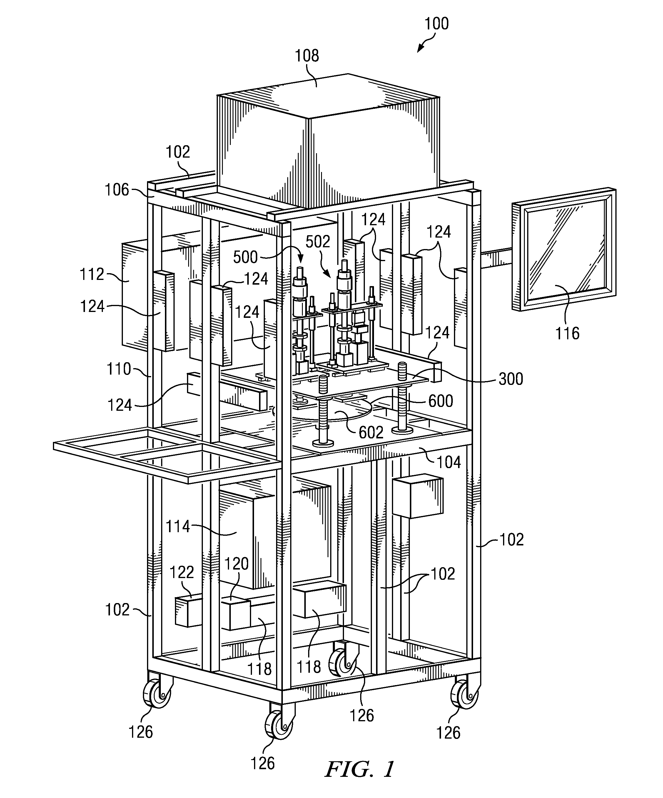
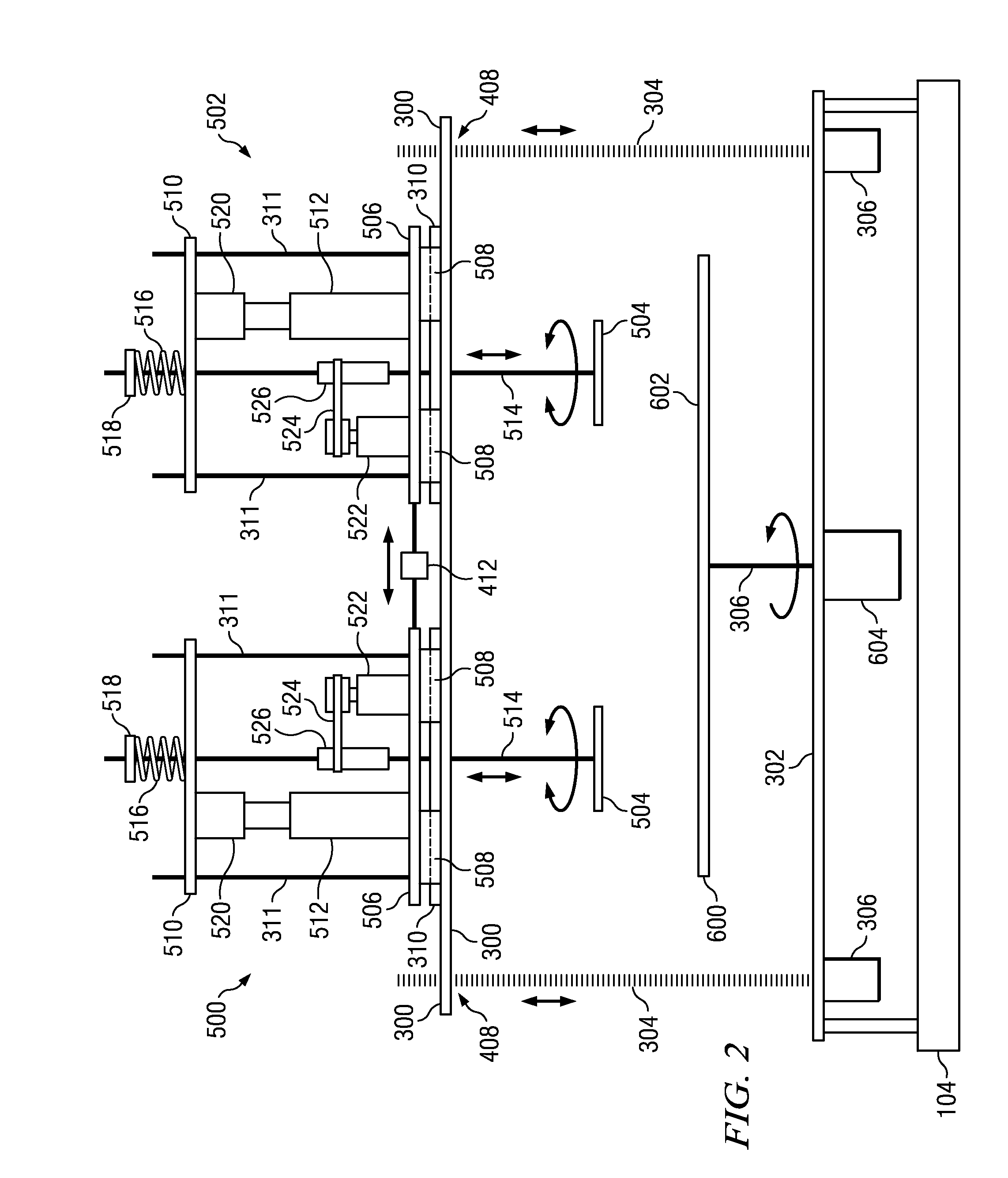
[0021]A polishing machine according to the invention, as installed in a supporting structural framework 100, is shown in FIG. 1. The frame 100 may be conveniently assembled from metal members 102 which may be made of steel, aluminum or similarly strong structural material. The frame 100 provides the structural support for the various machine components, such as the jig deck 300, polishing jigs 500, 502 and the polishing platen 600. The frame 100 includes a horizontal jig deck support grid 104 that, in the illustrated embodiment, is positioned approximately in the center of the frame 100. The jig deck support grid 104 provides structural support for the jig deck 300 (via a base and support shafts, later described) and indirectly the jigs 500, 502 and the polishing platen 600, and related equipment.

[0022]The main polishing machine components 300, 500, 502 and 600 are housed in a space extending from the support grid 104 up to a ceiling 106 formed of further structural members 102. Sin...


PUM


Abstract

At least one wafer is suspended on a respective jig shaft above a polishing platen. The degree of parallelism between the wafer and the polishing platen is controlled using a three-point suspension, which allows for planar pitch adjustments using vertical actuation algorithms. As the wafer is lowered into contact against the polishing platen, a load cell senses how much of the weight of the jig shaft, wafer mount and wafer continues to be supported by the jig. The vertical displacement of the wafer is controlled using a linear actuator responsive to a signal from the load cell. Vertical actuation of the wafer serves to increase or decrease this amount of supported weight, in turn decreasing or increasing the amount of applied down-force exerted between the wafer and the platen. A compression spring is used to increase the resolution of the pressure control. Finally, system components exposed to the work environment are encapsulated by chemically resistive components to prevent corrosion of system components.

Description

RELATED APPLICATIONS[0001]This application is a division of pending U.S. application Ser. No. 11 / 832,759, filed Aug. 2, 2007, the specification and drawings of which are fully incorporated by reference herein.BACKGROUND OF THE INVENTION[0002]Chemical polishing (CP) methods and apparatus have been known for many years. Prior art CP apparatus are directed to polishing the surfaces of relatively tough semiconductor materials such as those composed of elemental silicon. On such common semiconductor (and insulator) materials, one can exert appreciable pressure on the face to be polished without causing failure of the workpiece.[0003]Some semiconductor materials, particularly Group II-VI semiconductor materials and more particularly mercury cadmium telluride (MCT) and cadmium telluride (CT) materials, are more fragile and cannot withstand excessive downward pressure of the sort exerted in conventional polishing processes. By way of illustration, as measured on the Vickers scale, elemental...

Claims


Application Information

Patent Timeline
Patent Type & Authority Applications(United States)
IPC IPC(8): B24B49/16B24B51/00
CPCB24B37/005B24B49/16B24B37/30
Inventor CROCCO, JEROMESINGH, RASDIP
Owner DRS NETWORK & IMAGING SYST
Why Eureka
Try Eureka