Display device and electronic device including the same

a display device and electronic device technology, applied in the direction of diodes, optics, instruments, etc., can solve the problems of deterioration such as increased threshold voltage or decrease in mobility, driver circuit becomes difficult to operate, image cannot be displayed, etc., to achieve the effect of reducing the parasitic capacitance of the transistor reducing the number of transistors connected to the capacitor, and increasing the potential of a signal synchronizing with a clock signal

Active Publication Date: 2010-06-03
SEMICON ENERGY LAB CO LTD
View PDF19 Cites 85 Cited by
  • Summary
  • Abstract
  • Description
  • Claims
  • Application Information

AI Technical Summary

Benefits of technology

[0058]The number of transistors connected to a capacitor can be decreased. Alternatively, the parasitic capacitance of a transistor connected to the capacitor can be decreased. Alternatively, the potential in an H level of a signal which synchronizes with a clock signal can be increased. Alternatively, a layout area can be reduced. Alternatively, life can be extended. Alternatively, delay or distortion of a signal can be decreased. Alternatively, power consumption can be decreased. Alternatively, the adverse effect of noise can be decreased. Alternatively, deterioration of a transistor can be suppressed or relieved. Alternatively, malfunction can be suppressed. Alternatively, short circuit between one electrode of a capacitor and the other electrode of the capacitor can be prevented. Alternatively, the current driving capability of an outside circuit can be decreased. Alternatively, the size of an outside circuit can be reduced. Alternatively, the size of a display device can be reduced.

Problems solved by technology

However, deterioration such as increase in threshold voltage or decrease in mobility is caused in the transistor formed using the non-single-crystal semiconductor.
As the deterioration of the transistor advances, there is a problem in that the driver circuit becomes hard to operate and an image cannot be displayed.
However, in Patent Document 1, since the other electrode of the capacitor is connected to the gates of the two transistors, there is a problem in that the parasitic capacitance of a node connected to the capacitor is high.
Accordingly, there is a problem in that the potential in an H level of a signal that synchronizes with a clock signal becomes low.
In that case, there is a problem in that a time during which a transistor can be turned is shortened if the threshold voltage of the transistor increases.
That is, there is a problem in that the life of a shift register is shortened.
Alternatively, since the parasitic capacitance of the node connected to the capacitor is high, there is a problem in that the capacitance value of the capacitor should be large.
Accordingly, since an area where the one electrode of the capacitor and the other electrode of the capacitor overlap with each other needs to be large, there is a problem in that the layout area of the capacitor becomes large.
In Patent Document 1, since the area of the capacitor needs to be large, there is a problem in that short circuit between the one electrode and the other electrode tends to be caused due to dust or the like.
As a result, there is a problem in that yield is decreased and cost is increased.
In Patent Document 1, since the capacitance value of the capacitor needs to be large, there is a problem in that delay or distortion of a signal (e.g., a clock signal or an inverted clock signal) supplied to the capacitor becomes obvious.
Alternatively, there is a problem in that power consumption is increased.
Since a circuit having high current driving capability is used as a circuit for outputting a signal to be supplied to the capacitor, there is a problem in that an outside circuit (hereinafter also referred to as an external circuit) becomes large.
Alternatively, there is a problem in that a display device becomes large.
Accordingly, noise or the like is caused because the potential of the gate of the pull-up transistor Tu is not stable.
Therefore, there is a problem in that the shift register malfunctions.

Method used


Image

  • Display device and electronic device including the same
  • Display device and electronic device including the same
  • Display device and electronic device including the same

Examples


embodiment 1

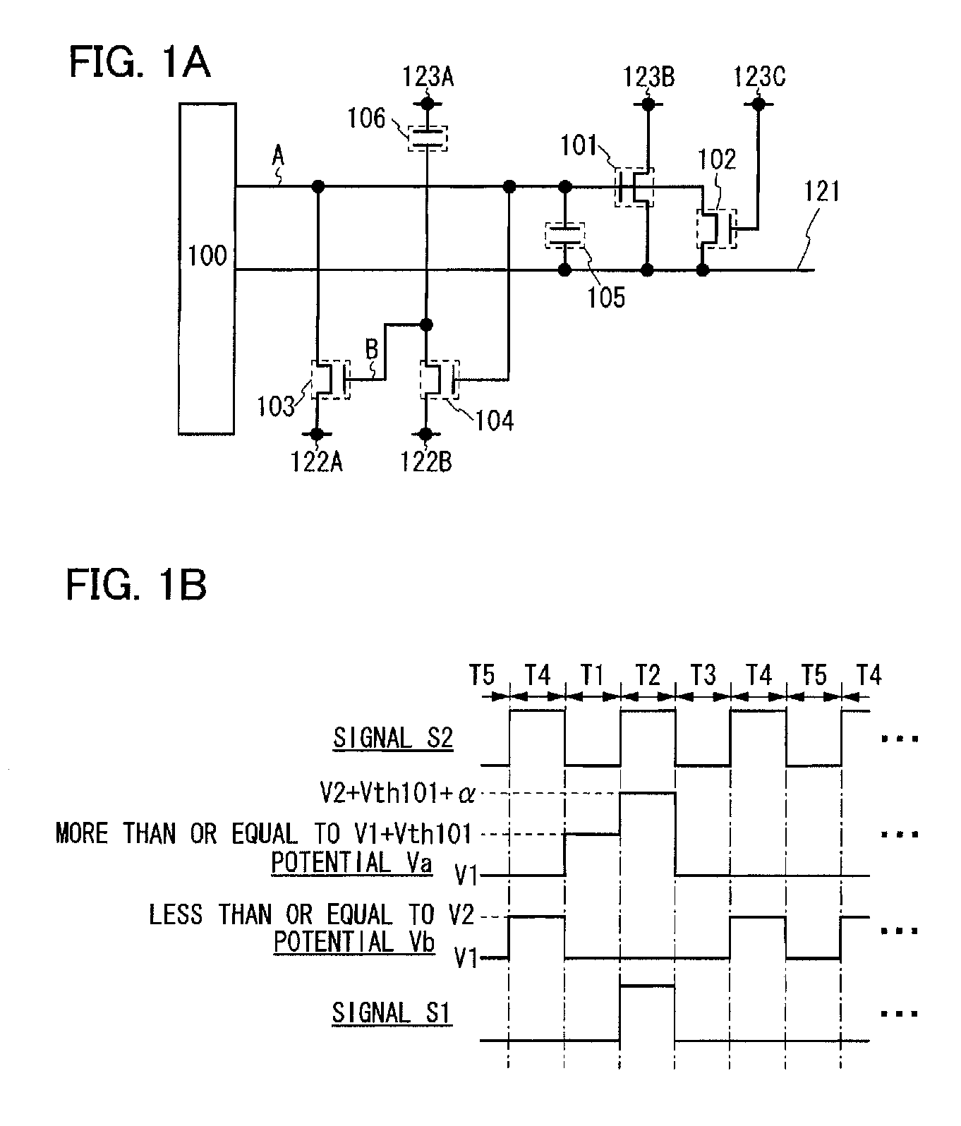
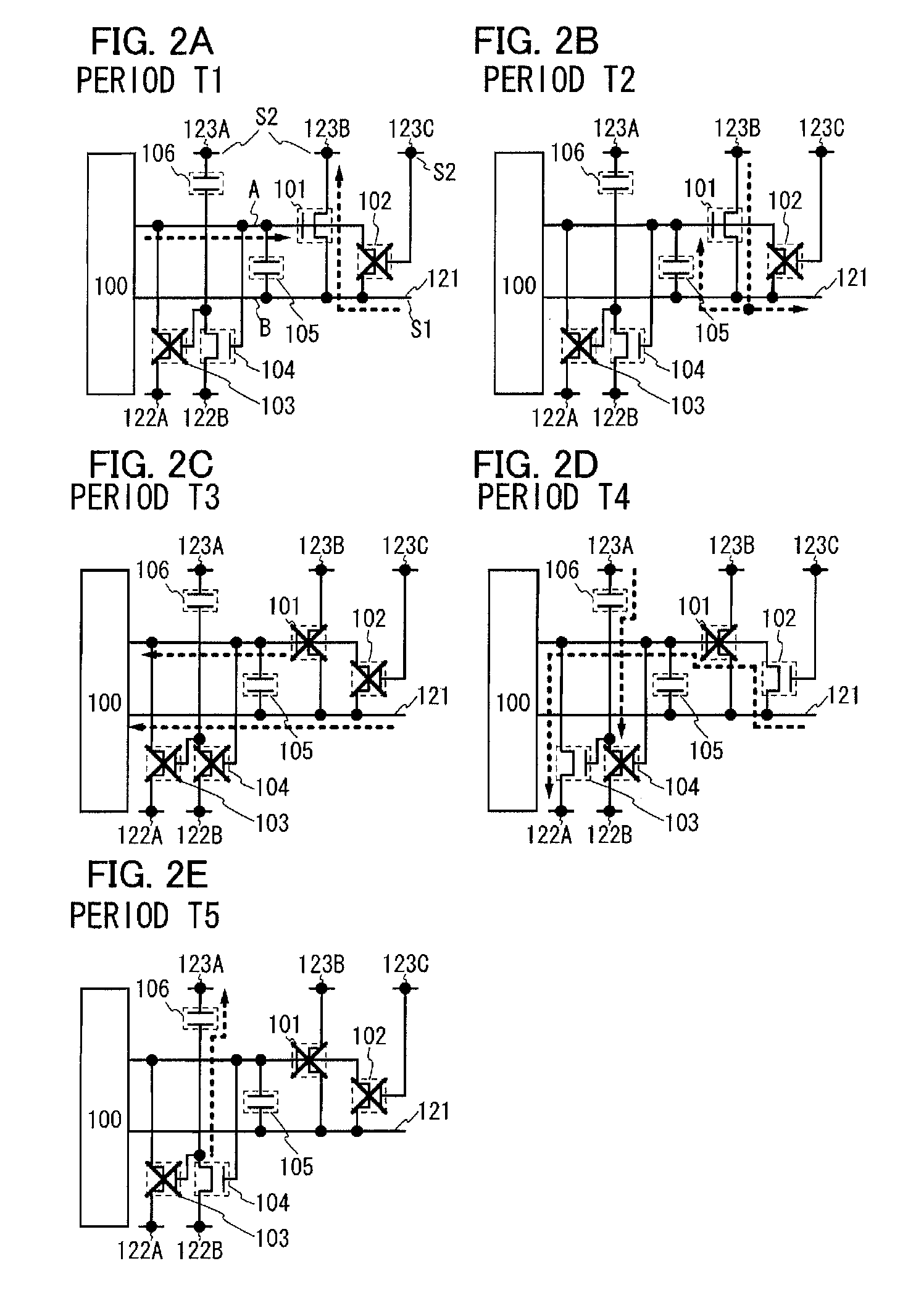
[0097]In this embodiment, one example of a semiconductor device will be described. Note that the semiconductor device can be denoted as a driver circuit or a flip-flop.

[0098]First, one example of the semiconductor device of this embodiment will be described with reference to FIG. 1A. The semiconductor device in FIG. 1A includes a circuit 100, a transistor 101, a transistor 102, a transistor 103, a transistor 104, a capacitor 105, and a capacitor 106. Each of the transistors 101 to 104 is an n-channel transistor which is turned on when potential difference (Vgs) between a gate and a source gets higher than threshold voltage (Vth). However, this embodiment is not limited to this. Each of the transistors 101 to 104 can be a p-channel transistor. The p-channel transistor is turned on when potential difference (Vgs) between a gate and a source gets lower than threshold voltage (Vth).

[0099]A connection relation of the semiconductor device in FIG. 1A will be described. A first terminal of ...

embodiment 2

[0174]In this embodiment, one example of the semiconductor device will be described. The semiconductor device of this embodiment is a specific example of the semiconductor device described in Embodiment 1. In specific, a specific example of the circuit 100 will be described in this embodiment. Note that the content described in Embodiment 1 can be applied to the semiconductor device in this embodiment.

[0175]The specific example of the circuit 100 will be explained with reference to FIG. 6A. However, FIG. 6A is one example and this embodiment is not limited to this. Circuits of a variety of structures can be used as the circuit 100 besides the circuit with the structure shown in FIG. 6A. Note that a portion which is similar to that in FIG. 1A is denoted by the same reference numeral and the description thereof is omitted.

[0176]The circuit 100 includes a transistor 131, a transistor 132, a transistor 133, a transistor 134, and a transistor 135. Each of the transistors 131 to 135 is an...

embodiment 3

[0235]In this embodiment, one example of a shift register is described. The shift register in this embodiment can include the semiconductor device of Embodiment 1 and Embodiment 2. Note that the shift register can also be referred to as a semiconductor device or a gate driver. Note that the content described in Embodiment 1 and Embodiment 2 can be applied to that of the shift register in this embodiment.

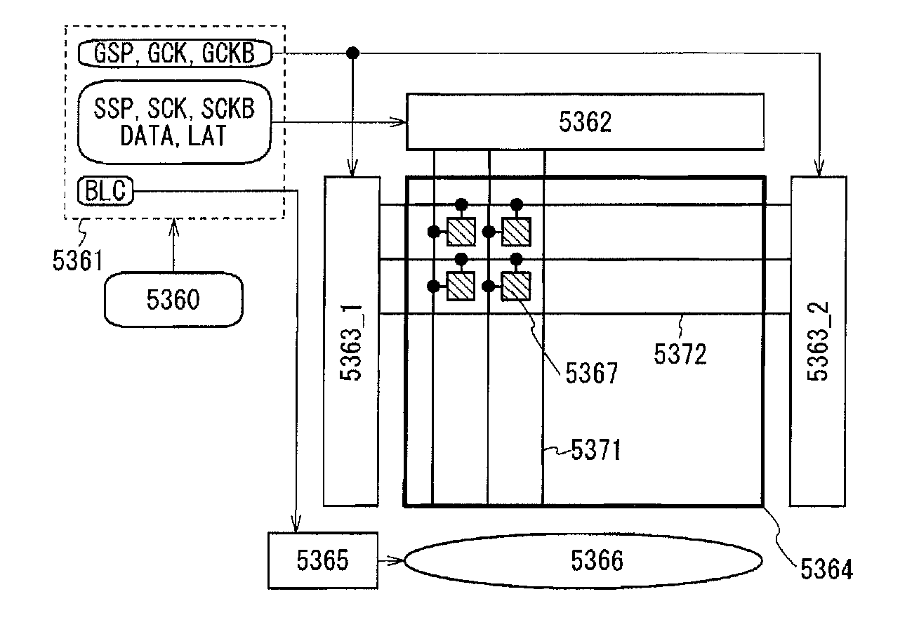
[0236]First, one example of the shift register will be described with reference to FIG. 14A. A shift register 220 is connected to wirings 201_1 to 201_N (N is a natural number), a wiring 202, a wiring 203, a wiring 204, a wiring 205, and a wiring 206.

[0237]The wiring 202 corresponds to the wiring 123 (the wirings 123A to 123C) described in Embodiment 1 and Embodiment 2 or the wiring 124 (the wirings 124A and 124B) described in Embodiment 1 and Embodiment 2 and can function as a signal line or a clock signal line. In addition, a signal GS2 is input from a circuit 221 to the wiring 202...


PUM

PropertyMeasurementUnit
currentaaaaaaaaaa
currentaaaaaaaaaa
currentaaaaaaaaaa

Abstract

It is an object to decrease the number of transistors connected to a capacitor. In a structure, a capacitor and one transistor are included, one electrode of the capacitor is connected to a wiring, and the other electrode of the capacitor is connected to a gate of the transistor. Since a clock signal is input to the wiring, the clock signal is input to the gate of the transistor through the capacitor. Then, on/off of the transistor is controlled by a signal which synchronizes with the clock signal, so that a period when the transistor is on and a period when the transistor is off are repeated. In this manner, deterioration of the transistor can be suppressed.

Description

TECHNICAL FIELD[0001]The present invention relates to a semiconductor device, a display device, a liquid crystal display device, a driving method thereof, or a producing method thereof. In specific, the present invention relates to a semiconductor device, a display device, or a liquid crystal display device including a driver circuit formed over the same substrate as a pixel portion, or a driving method of the device. Alternatively, the present invention relates to an electronic device including the device.BACKGROUND ART[0002]In recent years, with the increase of large display devices such as liquid crystal televisions, display devices have been actively developed. In specific, a technique of forming a driver circuit such as a gate driver over the same substrate as a pixel portion by using a transistor formed using a non-single-crystal semiconductor has been actively developed because the technique makes a great contribution for reduction in cost and improvement in reliability.[0003...

Claims


Application Information

Patent Timeline
Patent Type & Authority Applications(United States)
IPC IPC(8): G09G3/36G02F1/1368
CPCG09G3/3413G09G2310/0235H01L27/0629G09G2320/0252G02F1/136286G09G2310/061G02F1/13624G09G3/3266G09G3/3648G09G2310/0286
Inventor UMEZAKI, ATSUSHI
Owner SEMICON ENERGY LAB CO LTD
Why Eureka
Try Eureka