Carbon nanotube signal modulator and photonic transmission device

Active Publication Date: 2010-06-10
CARBON DESIGN INNOVATIONS
View PDF20 Cites 7 Cited by
  • Summary
  • Abstract
  • Description
  • Claims
  • Application Information

AI Technical Summary

Benefits of technology

[0010]The carbon nanotube (CNT) signal modulator comprises a gate CNT on a substrate in a position for (i) receiving an input photonic signal and an input modulation signal and (ii) transmitting an output photonic signal that is reduced, eliminated, or enhanced through the selection of the input modulation signal to provide a modulated output photonic signal; and an input modulation signal sender for sending the input modulat

Problems solved by technology

Electronic transistors are commonly fabricated on silicon wafers to make electronic computer chips and, unfortunately, have performance limitations that make them increasingly more expensive to manufacture to perform suitably as the performance requirements of computers increase.
Unfortunately, each of these attempts at pr

Method used


Image

  • Carbon nanotube signal modulator and photonic transmission device
  • Carbon nanotube signal modulator and photonic transmission device
  • Carbon nanotube signal modulator and photonic transmission device

Examples


example 1

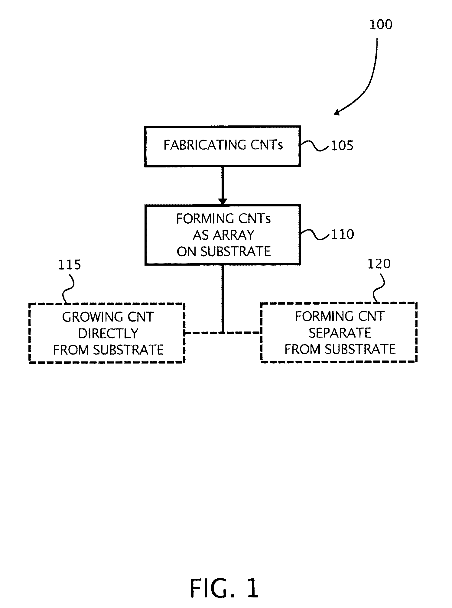
Controlled Manufacture of CNTs

[0048]The ability to manipulate nanomaterials in a controllable manner is needed for many nanotechnology applications. As-grown CNTs, for example, do not always exhibit the desired shape and configuration ideal for a given application but require further manipulation to render them suitable. In nanotransistors, the bends and kinks along the length of a CNT can change the bandgap of the CNT, thus altering its behavior. Modus Nanotechnology has fabricated multiple CNT nanoantenna geometries and orientations having lengths suitable for resonant interaction with photon wavelengths that range, for example, from the optical regime to the infrared. CNTs formed into functional geometries can perform as the functional element in a photonic device or as a nanoantenna.

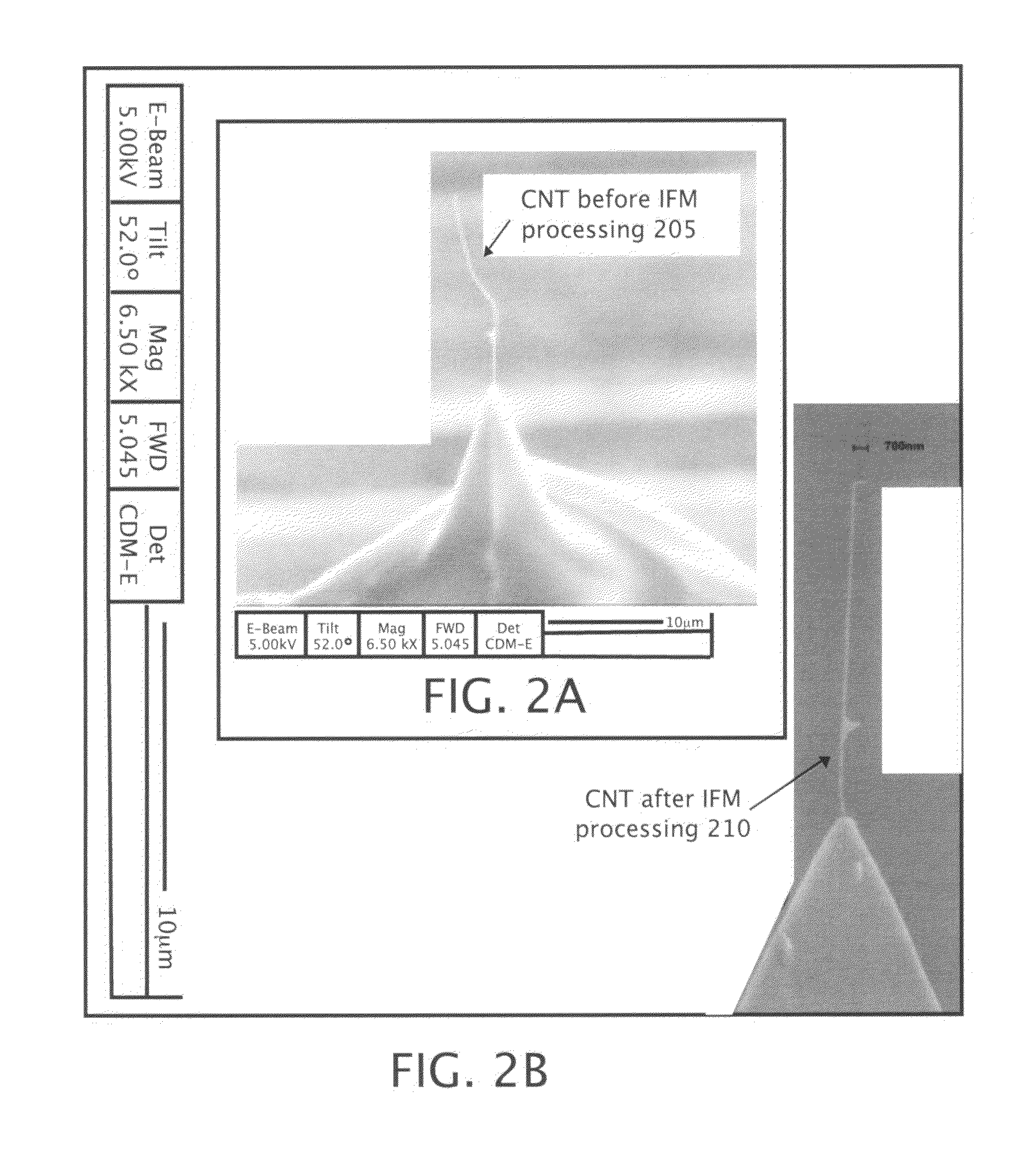
[0049]IBM (ion beam molding) can be used to create functional nanoantenna geometries. FIGS. 2A and 2B illustrate a CNT before and after IBM according to some embodiments of the present invention. In ...

example 2

CNT Nanoantennas

[0052]The performance metrics of the nanoantennas were tested and the results showed that CNTs fabricated into functional antenna forms, demonstrate photonic properties and antenna efficiencies comparable to theoretical values. Measured polarization proved dependent upon the orientation of the CNT and this property can lead to functional carbon nanotube based photonic logic device elements.

[0053]A nanotube acts as an antenna re-radiating light with an electric field E, polarized in the plane parallel to the CNT. A polarizer, with its axis of polarization rotated by an angle θ to this plane, transmits radiation with a projected electric field E′=E cos θ, and the corresponding observed intensity is given by the law of Malus INT=∝(E′)2=E2 cos θ. A general equation describing the scattering maxima from a random array of dipole antennas is:

L=m(λ2)f(θ,n)

where L is the scattered light, m is the ratio of the speed of electromagnetic propagation in the antenna to that in a va...

example 3

Measured Efficiency and Polarization Dependence of a CNT Nanoantenna

[0057]Example 2 shows the polarization relationship between the incident light and the light emitted from an oriented CNT. Since the polarized light must be coming from the CNT only, the emission data can be used to calculate the efficiency of a CNT nanoantenna. The E fields scattered by a cylinder can be expressed in a concise manner by resolving the incident and scattered fields into perpendicular and parallel components and consider the fields at large distances compared to its wavelength.

[0058]FIG. 4 illustrates polarization considerations for a CNT nanoantenna according to some embodiments. For unpolarized light incident on the cylinder axis, the scattered field, polarized parallel and perpendicular to the axis can be expressed in terms of the incident fields through the following matrix equation.

(EllsE⊥s)=3π2χtΩsinζk(rsinζ-zcosζ)(T1T4T3T2)(ElliE⊥i)

where χ and Ω are apparatus efficiency and scattering solid ang...


PUM


Abstract

The present invention contemplates a variety of methods and techniques for fabricating a carbon nanotube (CNT) signal modulator for reducing, eliminating, or enhancing the resonance interaction between photonic elements, and a photonic transmission device that may incorporate the signal modulator. The CNT signal modulator comprises a gate CNT on a substrate in a position for receiving an input photonic signal and an input modulation signal; and transmitting an output photonic signal that is reduced, eliminated, or enhanced through the selection of the input modulation signal; and an input modulation signal sender for sending the input modulation signal to the gate CNT and creating the modulated output photonic signal from the gate CNT. The photonic transmission device can contain a plurality of CNTs, each having functional antenna forms that are capable of a resonance interaction of photons between adjacent CNTs when formed as an array on a substrate. The photonic transmission device can also comprise the CNT signal modulator.

Description

BACKGROUND OF THE INVENTION[0001]1. Field of the Invention[0002]The invention pertains to a carbon nanotube signal modulator for reducing, eliminating, or enhancing the resonance interaction between photonic elements, and a photonic transmission device that may incorporate the signal modulator.[0003]2. Description of Related Art[0004]Electronic transistors are commonly fabricated on silicon wafers to make electronic computer chips and, unfortunately, have performance limitations that make them increasingly more expensive to manufacture to perform suitably as the performance requirements of computers increase. Photonic devices are under investigation as a potential solution to this problem—they are an advancement that takes advantage of the intrinsic properties of photons.[0005]Photonic computing serves as an example application. Photonic computing uses photons of laser light instead of electrons as the basis for the computing element. As a result of ongoing efforts in this field, th...

Claims


Application Information

Patent Timeline
IPC IPC(8): G02F3/00G02F1/00G02F1/21G02F1/061B05D5/06
CPCB82Y10/00G02F3/00Y10S977/932Y10S977/742H01L51/0048H10K85/221
Inventor STEVENS, RAMSEY M.
Owner CARBON DESIGN INNOVATIONS
Why Eureka
Try Eureka