Semiconductor storage device

a technology of semiconductor devices and storage devices, applied in semiconductor devices, digital storage, instruments, etc., can solve the problems of large number of defects, such as grain boundaries, in the pillar-shaped silicon layer, and the dram operation speed becomes slower, and achieves the effect of reducing resistan

Active Publication Date: 2010-06-10
UNISANTIS ELECTRONICS SINGAPORE PTE LTD
View PDF5 Cites 17 Cited by
  • Summary
  • Abstract
  • Description
  • Claims
  • Application Information

AI Technical Summary

Benefits of technology

[0016]According to a first aspect of the present invention, there is provided a semiconductor storage device designed using a vertical transistor which has a structure where a drain, a gate and a source are arranged in a vertical direction with respect to a pillar-shaped silicon layer, and a gate electrode is formed to surround the pillar-shaped silicon layer. The semiconductor storage device comprises a memory cell array formed with a plurality of first bit lines each comprised of a first layer and connected to a sense amplifier, and a plurality of second bit lines each comprised of a different layer from the first layer and connected to the sense amplifier. Each of the second bit lines has a lower resistance than that of the first bit line. In the memory cell array, a plurality of the vertical transistors are formed on each of the first bit lines, in a row, in such a manner as to allow the gate electrodes of the vertical transistors to serve as respective ones of a plurality of word lines each wired in a direction perpendicular to a corresponding one of the first bit lines. Further, each of the vertical transistors includes a first transistor for selecting an associated one of the memory cells, and a second transistor for connecting corresponding ones of the first bit lines and the second bit lines. The second transistor is adapted to be kept in its ON state during an operation of the storage device, whereby each of the first bit lines is backed with the corresponding one of the second bit lines to allow the first and second bit lines to form a substantially low-resistance bit line.

Problems solved by technology

Thus, along with progress of miniaturization, a DRAM operation speed becomes slower due to an increase in resistance of the bit line, to cause difficulty in achieving a DRAM operation speed required in the future.
However, this SGT-DRAM has the following problem.
The silicon is transformed into polysilicon through a heat treatment for forming a transistor, so that a large number of defects, such as grain boundaries, occur in the pillar-shaped silicon layer.
DRAM production yield is extremely sensitive to junction leak caused by defects in a transistor.
Thus, it is difficult to ensure sufficient production yield by the above production method.
As above, although the SGT-DRAM disclosed in the Patent Document 2 is capable of lowering a resistance of a bit line, it would be hardly practicable due to difficulty in ensuring sufficient production yield.
However, if the number of bit lines to be connected to one bit line is reduced to downsize a DRAM cell array, an extra area due to an increase in the number of peripheral circuits is increased to cause a significant increase in chip area.

Method used


Image

  • Semiconductor storage device
  • Semiconductor storage device
  • Semiconductor storage device

Examples


first embodiment

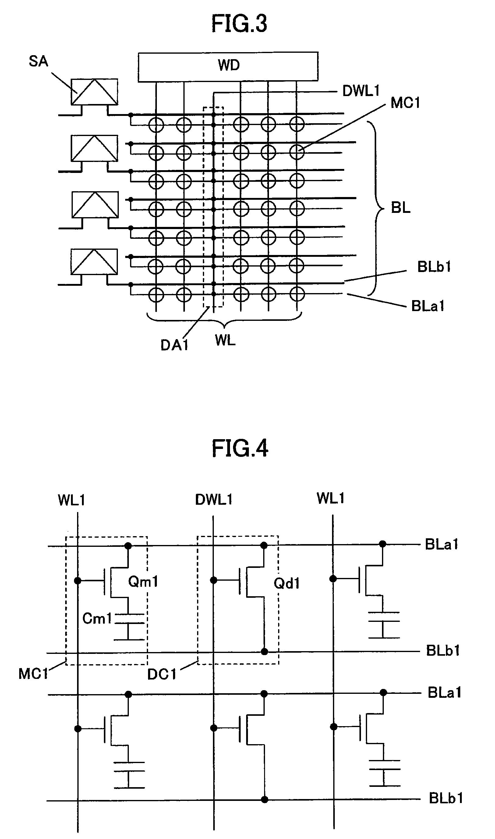
[0088]A first embodiment of the present invention shows an SGT-DRAM in which a structure and a layout configuration for a selection transistor and a capacitance element in a backing cell section are set to be exactly the same as those in a regular memory cell section, so that characteristics of a part of a plurality of regular memory cells adjacent to the backing cell section are not adversely affected (e.g., changed) by formation of the backing cell section.

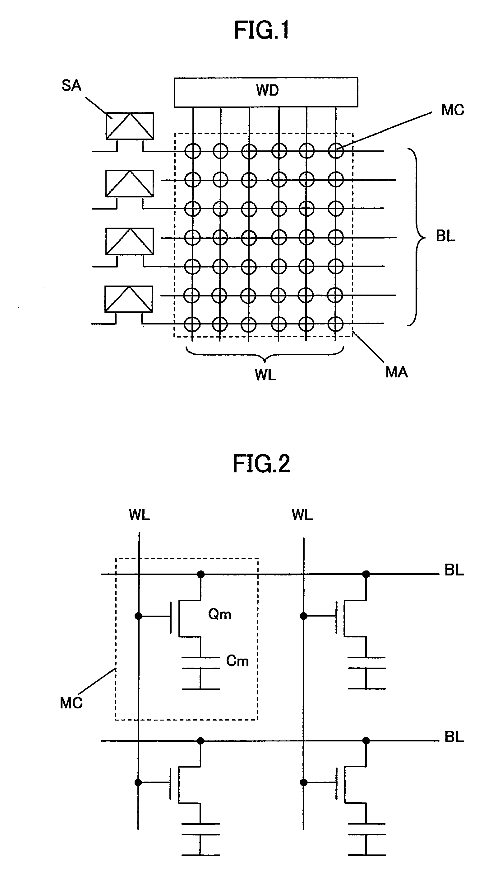
[0089]FIG. 1 shows an equivalent circuit of a memory cell array and a part of peripheral circuits in a conventional cross-point type SGT-DRAM. A memory cell is formed at each of all intersections of a plurality of bit lines BL and a plurality of word lines WL. Each of the bit lines is connected to a corresponding one of a plurality of sense amplifiers SA as a peripheral circuit, and the word lines are connected to a word driver WD as another peripheral circuit. FIG. 2 shows an equivalent circuit of the memory cell formed at one ...

second embodiment

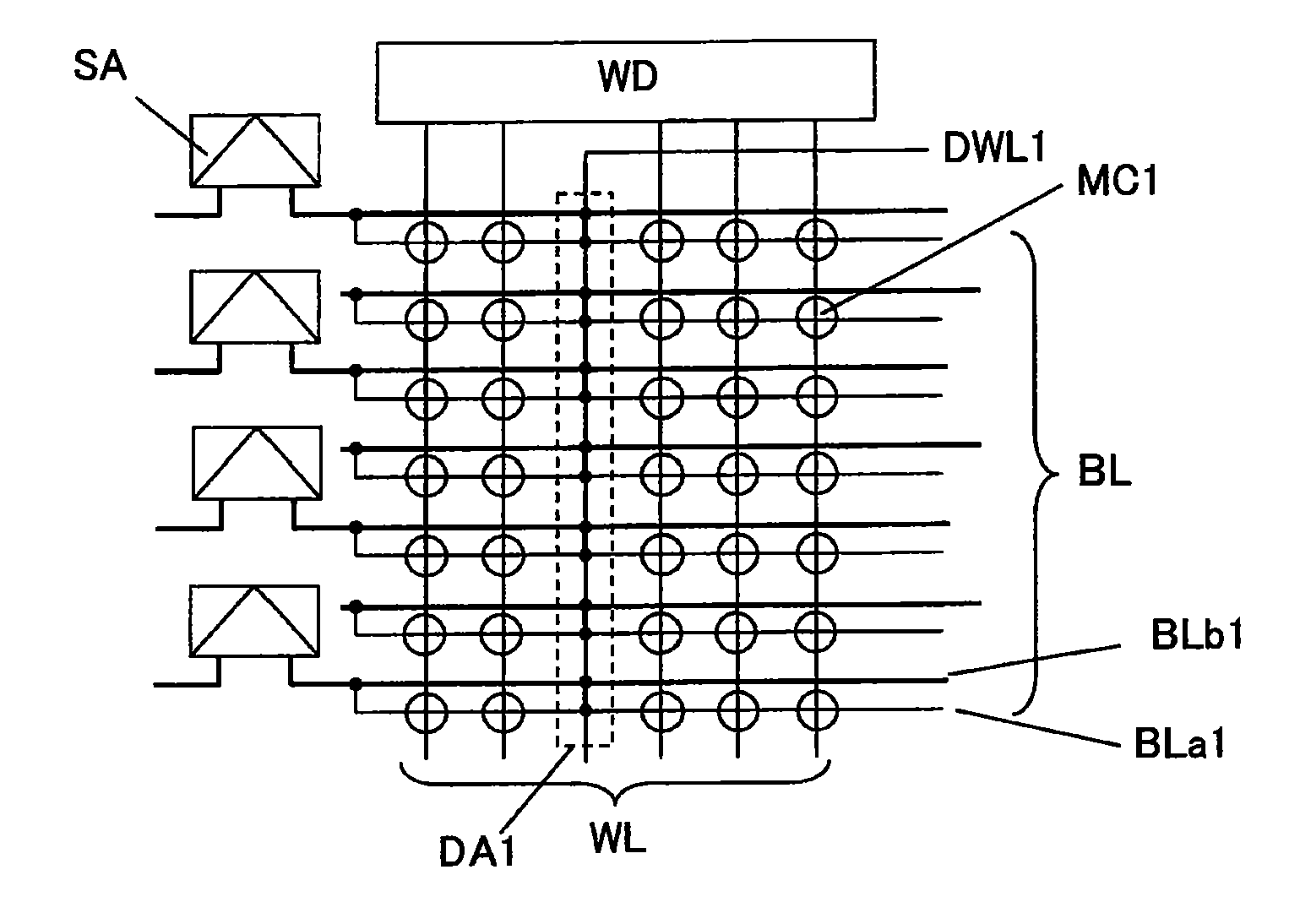
[0121]In the first embodiment, a high-resistance bit line is backed with a dedicated low-resistance bit-line layer formed within a memory cell array to provide a substantially low-resistance bit line. A second embodiment of the present invention shows an SGT-DRAM structure in which a high-resistance bit line comprised of a diffusion layer is backed with a first-layer interconnection line shared with a peripheral circuit. In the second embodiment, a need for forming a dedicated bit-line layer within a memory cell array can be eliminated to reduce the number of production steps.

[0122]Although a structure and a layout configuration for a transistor in a backing cell section is the same as those in a regular memory cell section, a structure and a layout configuration for a capacitance element becomes irregular in the backing cell section, because no capacitance element is formed in the backing cell section. Thus, characteristics of a capacitance element in a part of a plurality of regul...

third embodiment

[0138]A third embodiment of the present invention shows an SGT-DRAM structure in which a high-resistance bit line is backed with a low-resistance bit line through a pillar-shaped silicon layer comprised of a high-concentration N+ diffusion layer, instead of a backing transistor.

[0139]In the third embodiment, a high-resistance bit line is backed with a low-resistance bit line through a pillar-shaped silicon layer where a gate electrode and a gate dielectric film therearound are removed by etching, and an impurity is doped therein in a high concentration. Thus, a high-resistance bit line can be connected to a low-resistance bit line through a lower resistance than that in the first and second embodiments using a transistor.

[0140]FIG. 34 shows an equivalent circuit of a memory cell array and a part of peripheral circuits in an SGT-DRAM according to the third embodiment. As seen in this equivalent circuit, a plurality of high-resistance bit lines BLa3 each comprised of an N+ diffusion l...


PUM


Abstract

In a 4F2 memory cell designed using an SGT as a vertical transistor, a bit line has a high resistance because it is comprised of a diffusion layer underneath a pillar-shaped silicon layer, which causes a problem of slowdown in memory operation speed. The present invention provides a semiconductor storage device comprising an SGT-based 4F2 memory cell, wherein a bit line-backing cell having the same structure as that of a memory cell is inserted into a memory cell array to allow a first bit line composed of a diffusion layer to be backed with a low-resistance second bit line through the bit line backing cell, so as to provide a substantially low-resistance bit line, while suppressing an increase in area of the memory cell array.

Description

CROSS-REFERENCE TO RELATED APPLICATIONS[0001]Pursuant to 35 U.S.C. §119(e), this application claims the benefit of the filing date of Provisional U.S. Patent Application Ser. No. 61 / 207,599 filed on Feb. 13, 2009. This application is a continuation application of PCT / JP2009 / 051464 filed on Jan. 29, 2009 which claims priority under 35 U.S.C. §365(a) to PCT / JP2008 / 051299 filed on Jan. 29, 2008. The entire contents of these applications are hereby incorporated by reference.BACKGROUND OF THE INVENTION[0002]1. Technical Field[0003]The present invention relates to a semiconductor storage device and a production method therefor.[0004]2. Background Art[0005]With a view to achieving higher integration and higher performance of an LSI, an SGT (Surrounding Gate Transistor) has been proposed which is a vertical transistor comprising a pillar-shaped semiconductor layer formed on a surface of a semiconductor substrate, and a gate formed to surround a sidewall of the pillar-shaped semiconductor la...

Claims


Application Information

Patent Timeline
Patent Type & Authority Applications(United States)
IPC IPC(8): G11C11/24
CPCG11C11/4023H01L27/0207H01L27/10885H01L27/10876H01L27/10823H10B12/34H10B12/053H10B12/482
Inventor MASUOKA, FUJIOARAI
Owner UNISANTIS ELECTRONICS SINGAPORE PTE LTD
Why Eureka
Try Eureka