Display device

a display device and display technology, applied in the field of display devices, can solve the problems of low field effect mobility, deterioration of thin film transistors, low current, etc., and achieve the effects of reducing manufacturing costs of display devices, narrowing the frame size of display devices, and improving image display characteristics

Inactive Publication Date: 2010-06-17
SEMICON ENERGY LAB CO LTD
View PDF22 Cites 49 Cited by
  • Summary
  • Abstract
  • Description
  • Claims
  • Application Information

AI Technical Summary

Benefits of technology

[0023]Display characteristics of an image can be improved, and the frame size of a display device can be narrowed. Manufacturing cost of the display device can be reduced.

Problems solved by technology

A thin film transistor in which a channel formation region is formed using an amorphous silicon layer has problems such as low field effect mobility and low on current.
Further, when the thin film transistor is used for a long term, there are problems in that the thin film transistor is deteriorated, the threshold voltage is shifted, and on current is lowered.
On the other hand, a thin film transistor in which a channel formation region is formed using a microcrystalline silicon layer has a problem in that, whereas the field effect mobility is higher than that of the thin film transistor using an amorphous silicon layer, the off current is high, and thus sufficient switching characteristics cannot be obtained.
However, the thin film transistor in which a polycrystalline silicon layer is used for the channel formation region has a problem in that the manufacturing cost becomes higher than that of the thin film transistor using an amorphous silicon layer due to the necessity for a step of crystallizing a semiconductor layer.
For example, the laser annealing technique involved in the process for manufacturing a polycrystalline silicon layer has a problem in that the irradiated area with a laser beam is small and large-screen liquid crystal panels cannot be produced efficiently.

Method used


Image

  • Display device
  • Display device
  • Display device

Examples


embodiment 1

[0057]In this embodiment, n-channel thin film transistors forming a driver circuit are used as unipolar thin film transistors each including a microcrystalline semiconductor. As driver circuits for driving a pixel portion, an example of a source line driver circuit and / or an example of a gate line driver circuit are / is described, so that advantages of this embodiment will be described.

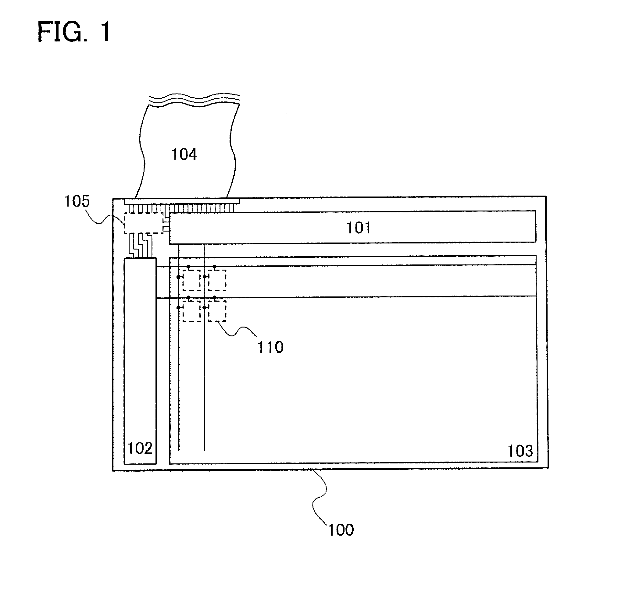
[0058]FIG. 1 illustrates an overall schematic view of a display device. A source line driver circuit 101, a gate line driver circuit 102, and a pixel portion 103 are formed together over a substrate 100. In the pixel portion 103, a portion surrounded by a dotted frame 110 corresponds to one pixel. FIG. 1 illustrates a structure in which the gate line driver circuit 102 is provided at one end portion; however, a plurality of gate line driver circuits 102 may be provided. In pixels of the display device, display elements are controlled by thin film transistors (hereinafter referred to as TFTs). Signals (...

embodiment 2

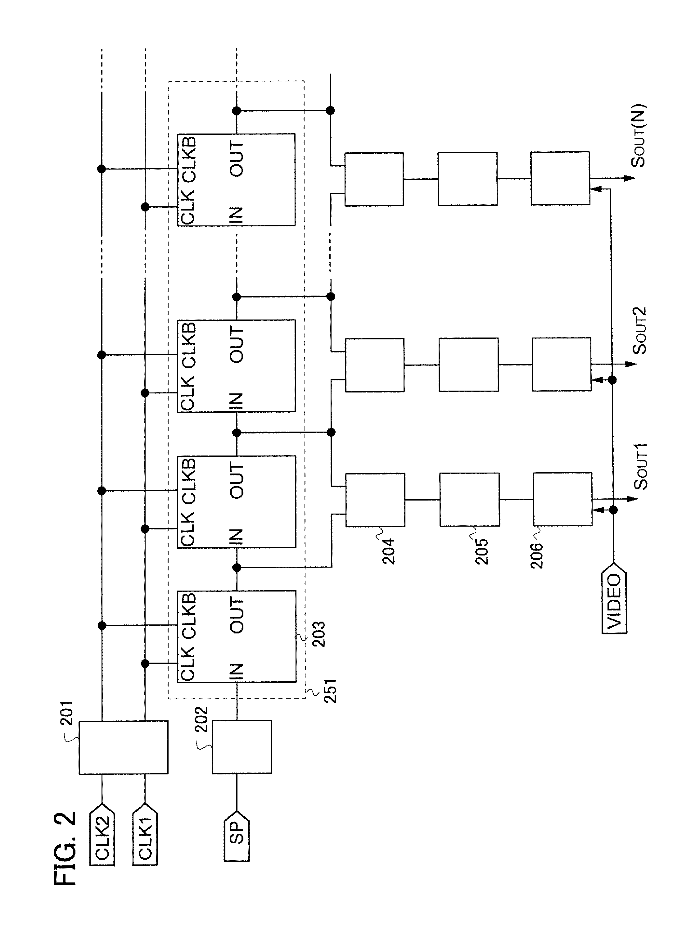
[0211]In the above embodiment, one example of a shift register formed using a static circuit as a shift register in a driver circuit of a display device is described. In this embodiment, one example of a driver circuit including a shift register formed using a dynamic circuit will be described.

[0212]A structure of a pulse output circuit included in a shift register formed using a dynamic circuit will be described with reference to FIGS. 17A to 17D. A pulse output circuit 1400 illustrated in FIG. 17A includes, as one example, an inverter circuit 1401 to which a start pulse SP is input from an input terminal, a switch 1402 whose one terminal is connected to an output terminal of the inverter circuit 1401, and a capacitor 1403 which is connected to the other terminal of the switch 1402. Note that on / off of the switch 1402 of the pulse output circuits of odd-numbered stages is controlled by the first clock signal (CLK1). Further, on / off of the switch 1402 of the pulse output circuits of...

embodiment 3

[0222]In this embodiment, a basic structure of a shift register of a display device with less variation in a threshold voltage will be described with reference to drawings. FIG. 19 illustrates a flip-flop of one stage (e.g., a first stage), which is one of a plurality of flip-flops included in a shift register.

[0223]The flip-flop shown in FIG. 19 includes a first thin film transistor 1301, a second thin film transistor 1302, a third thin film transistor 1303, a fourth thin film transistor 1304, and a fifth thin film transistor 1305. Note that the flip-flop is connected to a first wiring 1311, a second wiring 1312, a third wiring 1313, a fourth wiring 1314, a fifth wiring 1315, a sixth wiring 1316, and a seventh wiring 1317. In this embodiment, the fifth thin film transistor 1305 is an n-channel thin film transistor and is turned on when gate-source voltage (Vgs) exceeds the threshold voltage (Vth). Note that the seventh wiring 1317 may be called a third signal line.

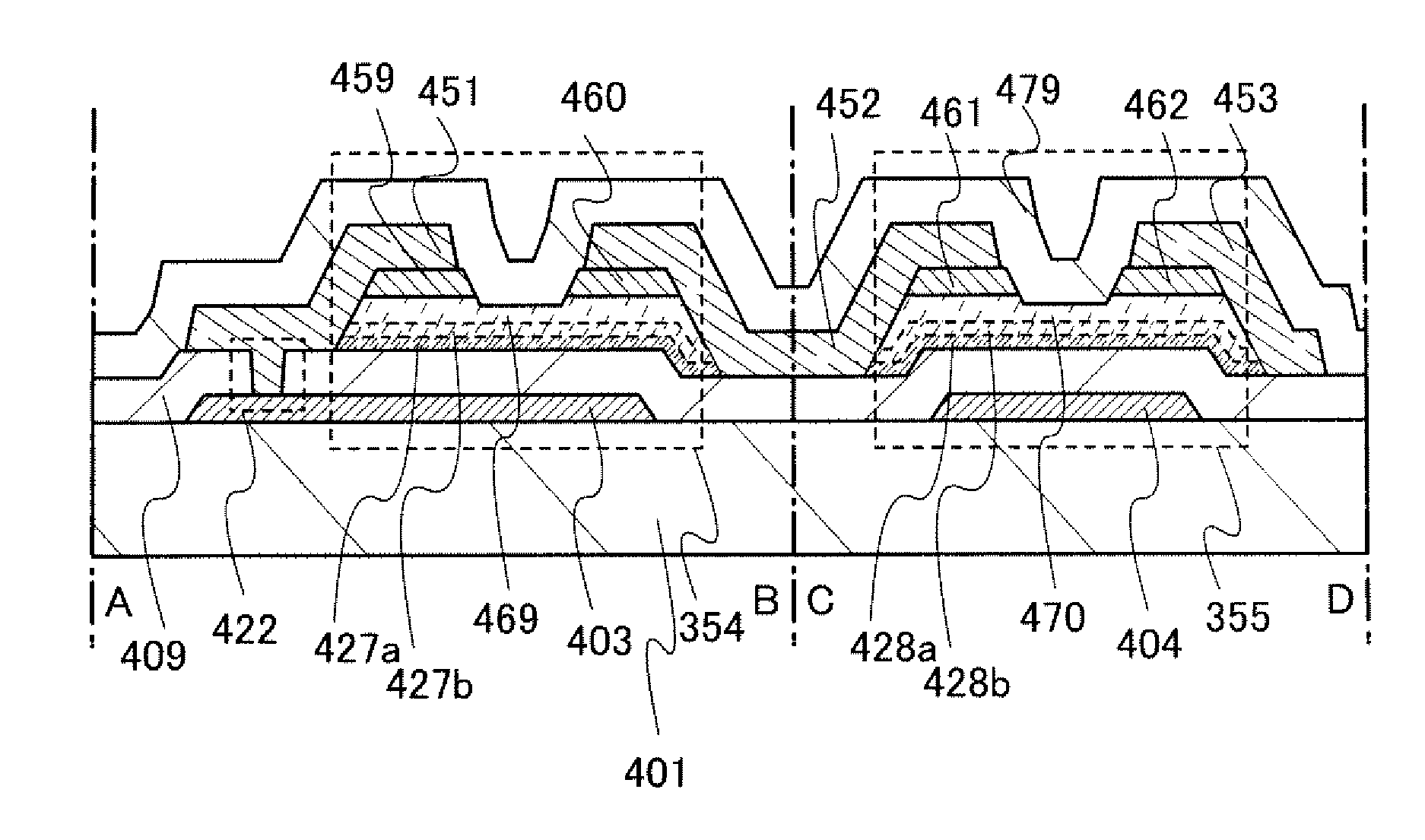
[0224]A first ter...


PUM


Abstract

A display device including an inverter circuit and a switch is provided. The inverter circuit includes a first thin film transistor and a second thin film transistor which have the same conductivity type. The first thin film transistor and the second thin film transistor each include: a gate insulating layer in contact with a gate electrode; a microcrystalline semiconductor layer in contact with the gate insulating layer; a mixed layer in contact with the microcrystalline semiconductor layer; a layer which includes an amorphous semiconductor and is in contact with the mixed layer; and a wiring. A conical or pyramidal microcrystalline semiconductor region and an amorphous semiconductor region filling a space except the conical or pyramidal microcrystalline semiconductor region are included in the mixed layer.

Description

BACKGROUND OF THE INVENTION[0001]1. Field of the Invention[0002]The present invention relates to a display device including an inverted staggered thin film transistor in each of a driver circuit and a pixel portion.[0003]2. Description of the Related Art[0004]As one kind of field-effect transistor, a thin film transistor in which a channel formation region is formed using a semiconductor layer formed over a substrate having an insulating surface is known. Techniques in which amorphous silicon, microcrystalline silicon, or polycrystalline silicon is used for the semiconductor layer used in the thin film transistor have been disclosed. A typical application of thin film transistors is a liquid crystal television device, in which thin film transistors have been put to practical use as a switching transistor for each pixel that constitutes a display screen.[0005]Further, for reduction in cost of a display device, there is a display device whose number of external components is reduced a...

Claims


Application Information

Patent Timeline
Patent Type & Authority Applications(United States)
IPC IPC(8): H01L33/00
CPCH01L29/78696H01L27/1222H01L29/04
Inventor KOYAMA, JUNMIYAIRI, HIDEKAZU
Owner SEMICON ENERGY LAB CO LTD
Why Eureka
Try Eureka