Method for producing group iii nitride semiconductor crystal, group iii nitride semiconductor substrate, and semiconductor light- emitting device

a technology of nitride and semiconductor crystals, which is applied in the direction of polycrystalline material growth, crystal growth process, chemically reactive gas, etc., can solve the problems of difficult to grow a compound bulk crystal according to a conventional melt growth method or the like, piezoelectric field formation, internal quantum efficiency reduction, etc., and achieve high quality and free from defects.

Inactive Publication Date: 2010-06-17
MITSUBISHI CHEM CORP
View PDF21 Cites 33 Cited by
  • Summary
  • Abstract
  • Description
  • Claims
  • Application Information

AI Technical Summary

Benefits of technology

[0017]According to the invention, for example, there is provided an advantageous method for producing a group III nitride semiconductor crystal having high quality and having a large-area non-polar plane. In the group III nitride semiconductor crystal of the invention, there exist no dislocation line parallel to the surface thereof, and the crystal has high quality and is free from a defect as influenced by the crystal morphology of the underlying base structure, and therefore, for example, the crystal is favorable as a substrate for light-emitting device applications.

Problems solved by technology

However, the nitrogen equilibrium vapor pressure over GaN is extremely high as compared with that over Ga, and therefore, it is difficult to grow a bulk crystal of the compound according to a conventional melt growth method or the like.
In InGaN-based blue and green LED and LD comprising a GaN substrate in which the C-plane is the surface thereof, there is a problem in that a piezoelectric field forms in the growth axis direction, or that is, in the C-axis direction thereof.
As a result, the internal quantum efficiency lowers, therefore reducing the external quantum efficiency in light-emitting devices.
However, Patent Reference 1 does not disclose a method for producing substrates.

Method used


Image

  • Method for producing group iii nitride semiconductor crystal, group iii nitride semiconductor substrate, and semiconductor light- emitting device
  • Method for producing group iii nitride semiconductor crystal, group iii nitride semiconductor substrate, and semiconductor light- emitting device
  • Method for producing group iii nitride semiconductor crystal, group iii nitride semiconductor substrate, and semiconductor light- emitting device

Examples


example 1

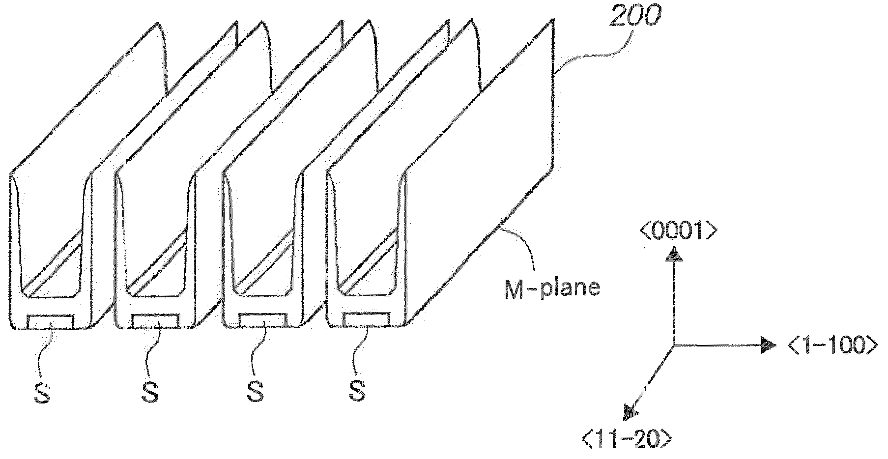
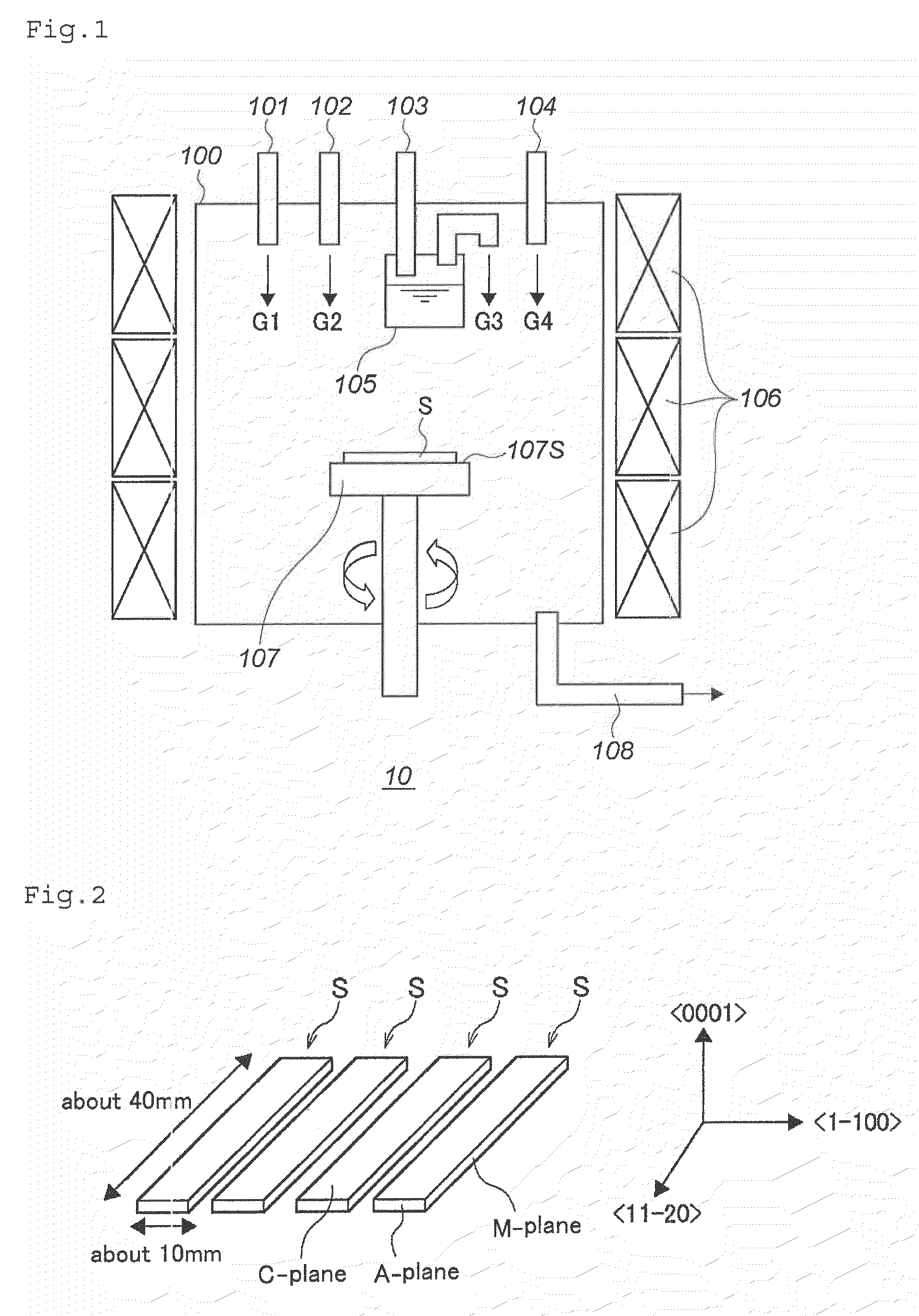
[0064]As seed crystal S, four bar-shaped free-standing GaN substrates graphically shown in FIG. 2 (hereinafter referred to as GaN seed crystal) were prepared. The GaN seed crystal S is a rectangular body designed as follows: Its periphery is formed of a straight line, the {0001} plane (that is, the C-plane) is the main plane, the M-plane is the long side plane, and the A-plane is the short side plane. The long side plane is planed by cleavage. Regarding the size, the long side is about 40 mm, the short side is about 10 mm, and the thickness is about 400 μm.

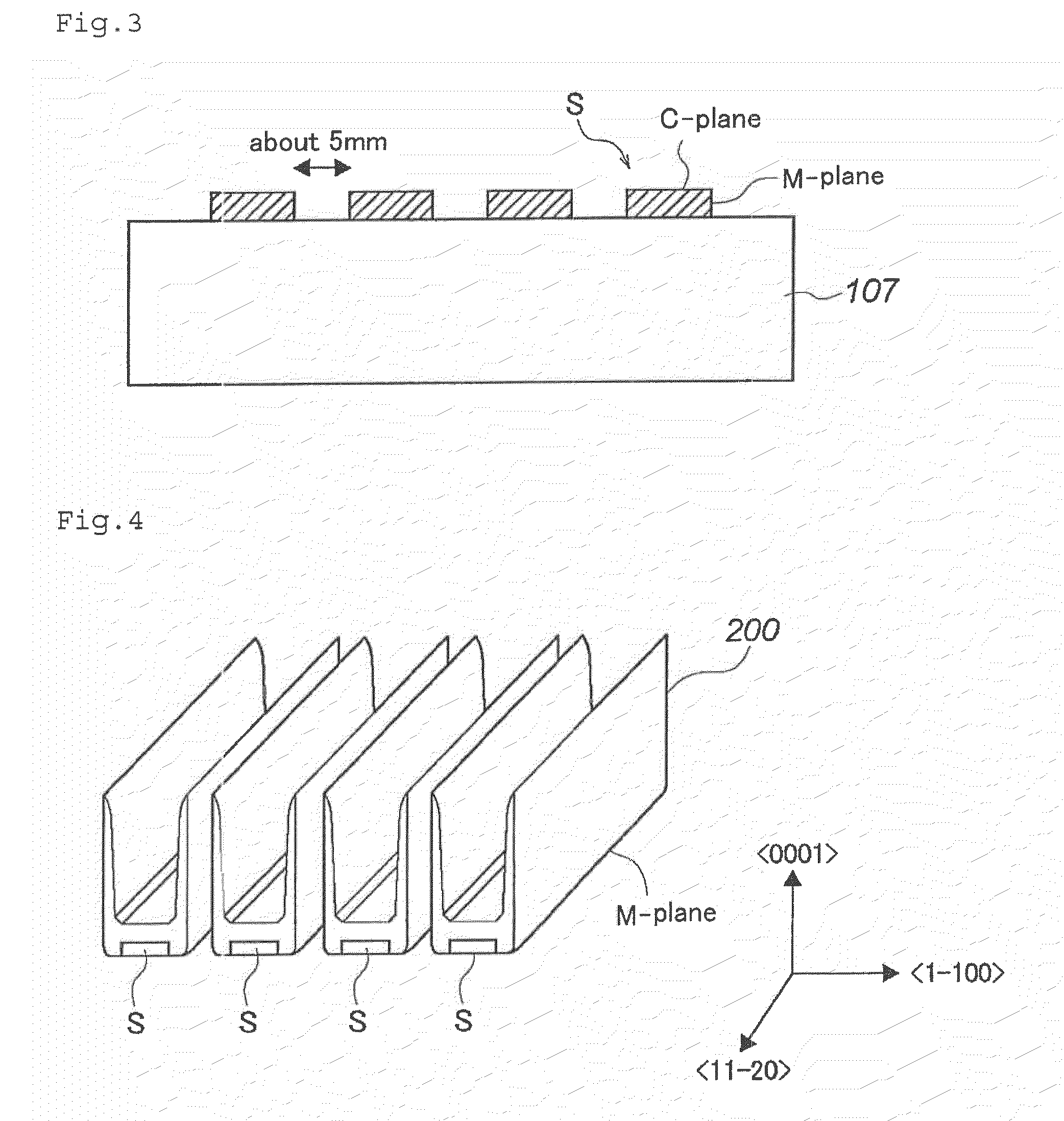
[0065]As the supporting head 107 in the HVPE device 10 shown in FIG. 1, employed was an SiC-coated carbon-made supporting head having a diameter of 80 mm and a thickness of 20 mm. As illustrated in FIG. 3, four GaN seed crystals S were put on the supporting head 107 as spaced from each other by an interval of about 5 mm, and processed for a growing step of GaN crystal thereon, as follows:

[0066]The reaction chamber 100 in the HVPE ...

example 2

[0072]As seed crystal S, four bar-shaped free-standing GaN substrates (hereinafter referred to as GaN seed crystal) were prepared. The GaN seed crystal S is a rectangular body designed as follows: The (0001) plane (that is, the C-plane) is the main plane, the plane inclined by 0.2° in the A-axis direction relative to the M-plane is the long side plane, and the A-plane is the short side plane. Regarding the size, the long side is about 40 mm, the short side is about 10 mm, and the thickness is about 400 μm.

[0073]The supporting of the GaN seed crystal S by the supporting head 107, and the temperature, the gas partial pressure and the growing time in the growing step for GaN crystal were the same as in Example 1. After the growing step for GaN crystal, the system was cooled to room temperature to give a GaN crystal.

[0074]Like in Example 1, the structure of the obtained GaN crystal had a wall part, as graphically shown in FIG. 4. Cutting out from the wall part gave a rectangular bulk cr...

example 3

[0076]As seed crystal S, four bar-shaped free-standing GaN substrates (hereinafter referred to as GaN seed crystal) were prepared. The GaN seed crystal S is a rectangular body designed as follows: The (0001) plane (that is, the C-plane) is the main plane, the plane inclined by 0.4° in the A-axis direction relative to the M-plane is the long side plane, and the A-plane is the short side plane.

[0077]The supporting of the GaN seed crystal S by the supporting head 107, and the temperature, the gas partial pressure and the growing time in the growing step for GaN crystal were the same as in Example 1. After the growing step for GaN crystal, the system was cooled to room temperature to give a GaN crystal.

[0078]As graphically shown in FIG. 9, the GaN crystal 200′ obtained in the above-mentioned growing step is the same as in Examples 1 and 2 in that it has a wall part extending from the M-plane of the GaN seed crystal S in the +C-axis direction ( direction) thereof. However, in Example 3, ...


PUM

PropertyMeasurementUnit
off angleaaaaaaaaaa
off angleaaaaaaaaaa
areaaaaaaaaaaa

Abstract

The method for producing a group III nitride semiconductor crystal of the invention comprises a step of preparing a seed crystal having a non-polar plane followed by growing a group III nitride semiconductor from the non-polar plane in a vapor phase, wherein the growing step includes growing the group III nitride semiconductor so as to extend in the +C-axis direction of the seed crystal. A group III-V nitride semiconductor crystal having high quality and a large-area non-polar plane can be obtained by the method.

Description

TECHNICAL FIELD[0001]The present invention relates to a method for producing a group III nitride semiconductor crystal such as GaN (gallium nitride), a group III nitride semiconductor substrate and a semiconductor light-emitting device.BACKGROUND ART[0002]A group III nitride single crystal such as typically gallium nitride (GaN) is useful as a substance applicable to light-emitting devices such as light-emitting diodes, laser diodes, etc., and high-frequency high-power electronic devices such as HEMT, HBT, etc. Accordingly, it is needed to efficiently produce a group III nitride semiconductor crystal such as GaN or the like of high crystallinity.[0003]For example, a most ideal substrate usable for growth of a GaN crystal thereon is a GaN substrate. However, the nitrogen equilibrium vapor pressure over GaN is extremely high as compared with that over Ga, and therefore, it is difficult to grow a bulk crystal of the compound according to a conventional melt growth method or the like. A...

Claims


Application Information

Patent Timeline
Patent Type & Authority Applications(United States)
IPC IPC(8): H01L33/32H01L21/20H01L29/20H01L33/16
CPCC30B25/20H01L31/1848H01L21/0237H01L21/02433H01L21/0254H01L21/02609H01L21/0262H01L21/02645H01L29/045H01L29/2003H01L33/16H01L33/18H01L33/32H01L33/00C30B29/403C30B29/38
Inventor FUJITO, KENJIKIYOMI, KAZUMASA
Owner MITSUBISHI CHEM CORP
Why Eureka
Try Eureka