Polycrystalline group iii metal nitride with getter and method of making

a metal nitride and polycrystalline technology, applied in the field of polycrystalline group iii metal nitride with getter and making method, crystalline nitride material, can solve the problems of crystal coloration, poor optoelectronic device performance, and difficulty in providing bulk layer of gan material, so as to achieve cost-effective, simple and cost-effective manufacturing

Active Publication Date: 2010-06-17
SLT TECH
View PDF101 Cites 265 Cited by
  • Summary
  • Abstract
  • Description
  • Claims
  • Application Information

AI Technical Summary

Benefits of technology

[0013]Benefits are achieved over pre-existing techniques using the present invention. In particular, the present invention enables a cost-effective manufacture of crystals that serve as a starting material for high quality gallium nitride containing crystal growth. In a specific embodiment, the present method and apparatus can operate with components that are relatively simple and cost effective to manufacture, such as ceramic and steel tubes. A specific embodiment also takes advantage of a getter material suitable for processing one or more chemicals for manufacture of high quality gallium nitride starting material. Depending upon the embodiment, the present apparatus and method can be manufactured using conventional materials and / or methods according to one of ordinary skill in the art. In preferred embodiments, the final crystal structure is substantially clear and free of haze and other features that may be undesirable. Depending upon the embodiment, one or more of these benefits may be achieved. These and other benefits may be described throughout the present specification and more particularly below.

Problems solved by technology

Although successful, conventional growth rates achieved make it difficult to provide a bulk layer of GaN material.
Additionally, dislocation densities are also high and lead to poorer optoelectronic device performance.
An ongoing challenge of ammonothermally-grown GaN crystals is a significant level of impurities, which cause the crystals to be colored, e.g., yellowish, greenish, grayish, or brownish.
The residual impurities may cause optical absorption in light emitting diodes fabricated on such substrates, negatively impacting efficiency, and may also degrade the electrical conductivity and / or generate stresses within the crystals.

Method used


Image

  • Polycrystalline group iii metal nitride with getter and method of making
  • Polycrystalline group iii metal nitride with getter and method of making
  • Polycrystalline group iii metal nitride with getter and method of making

Examples


Embodiment Construction

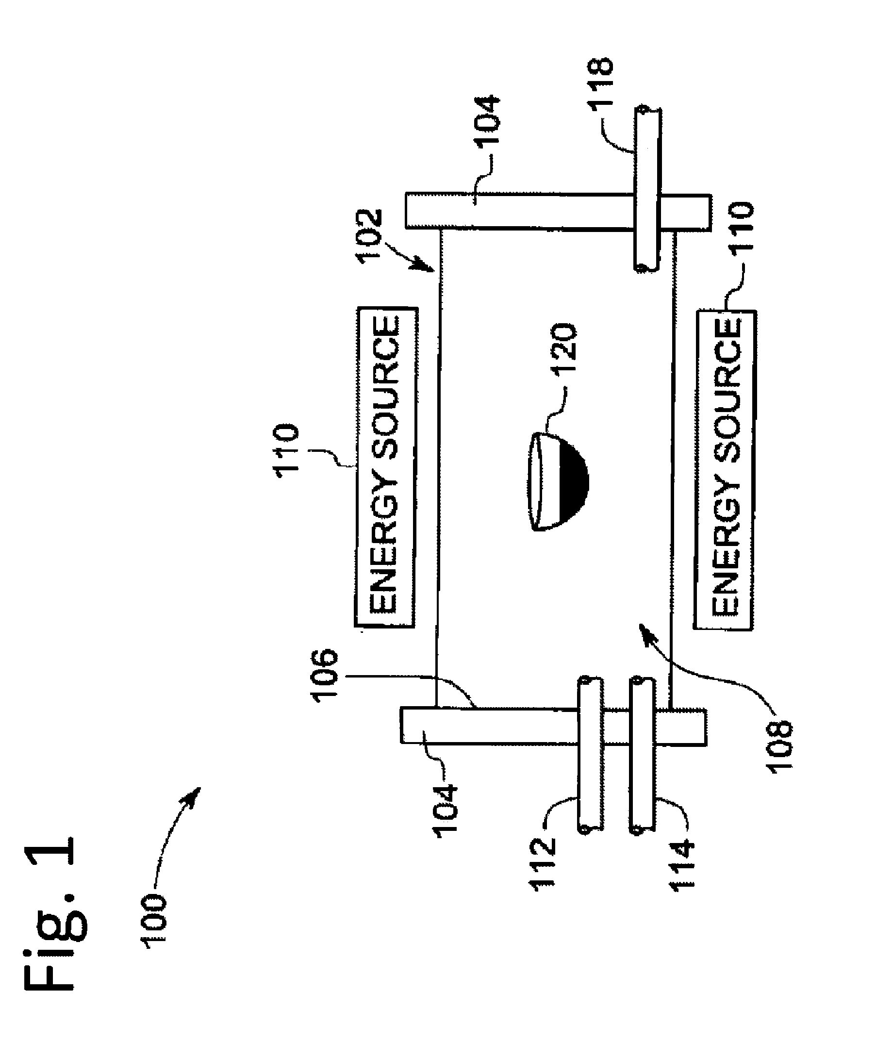
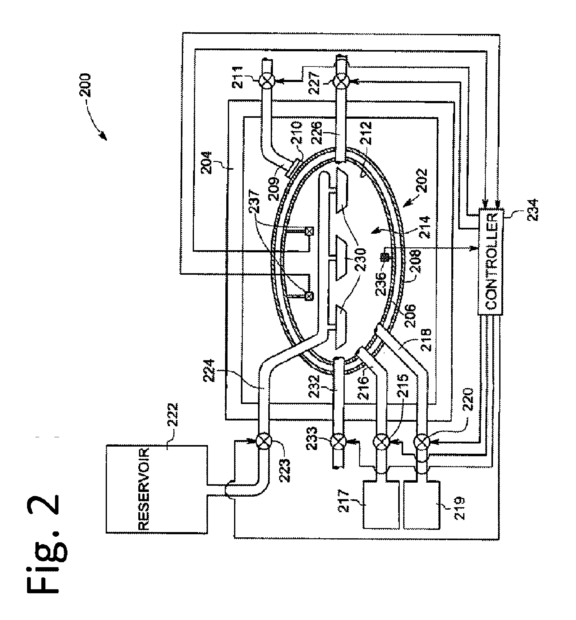
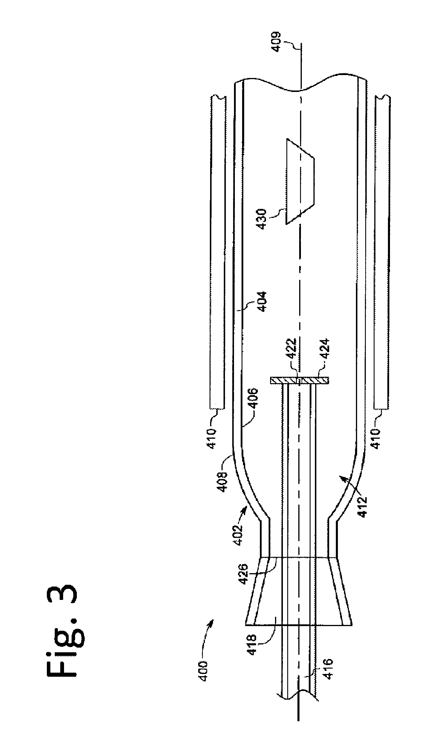
[0018]According to the present invention, techniques related to processing of materials for growth of crystals are provided. More particularly, the present invention provides a crystalline nitride material suitable for use as a raw material for crystal growth of a gallium-containing nitride crystal by an ammonobasic or ammonoacidic technique, but there can be others. In other embodiments, the present invention provides methods suitable for synthesis of polycrystalline nitride materials, but it would be recognized that other crystals and materials can also be processed. Such crystals and materials include, but are not limited to, GaN, AlN, InN, InGaN, AlGaN, and AlInGaN, and others for manufacture of bulk or patterned substrates. Such bulk or patterned substrates can be used for a variety of applications including optoelectronic devices, lasers, light emitting diodes, solar cells, photoelectrochemical water splitting and hydrogen generation, photodetectors, integrated circuits, and t...


PUM

PropertyMeasurementUnit
average grain sizeaaaaaaaaaa
porosityaaaaaaaaaa
porosityaaaaaaaaaa

Abstract

A gettered polycrystalline group III metal nitride is formed by heating a group III metal with an added getter in a nitrogen-containing gas. Most of the residual oxygen in the gettered polycrystalline nitride is chemically bound by the getter. The gettered polycrystalline group III metal nitride is useful as a raw material for ammonothermal growth of bulk group III nitride crystals.

Description

CROSS-REFERENCES TO RELATED APPLICATIONS[0001]This application claims priority to Provisional Patent Application No. 61 / 122,332, filed Dec. 12, 2008, commonly assigned, and incorporated by reference herein for all purpose.BACKGROUND OF THE INVENTION[0002]The present invention generally relates to processing of materials for growth of crystals. More particularly, the present invention provides a crystalline nitride material suitable for use as a raw material for crystal growth of a gallium-containing nitride crystal by an ammonobasic or ammonoacidic technique, but there can be others. In other embodiments, the present invention provides methods suitable for synthesis of polycrystalline nitride materials, but it would be recognized that other crystals and materials can also be processed. Such crystals and materials include, but are not limited to, GaN, AlN, InN, InGaN, AlGaN, and AlInGaN, and others for manufacture of bulk or patterned substrates. Such bulk or patterned substrates can...

Claims


Application Information

Patent Timeline
Patent Type & Authority Applications(United States)
IPC IPC(8): H01J7/18H01B1/06B32B9/00B32B5/14
CPCC30B9/00Y10T428/24355C30B29/403C30B28/06
Inventor D'EVELYN, MARK P.
Owner SLT TECH
Why Eureka
Try Eureka