Carrier for transmitting high frequency signal and carrier layout method thereof

a carrier and high frequency technology, applied in the field of signal transmission, can solve the problems of affecting the requirement of signal quality, increasing the area, and the inability of low-pass filter operation, and achieve the effect of increasing high-frequency loss and flexible design

Active Publication Date: 2010-06-24
ASKEY COMP
View PDF6 Cites 12 Cited by
  • Summary
  • Abstract
  • Description
  • Claims
  • Application Information

AI Technical Summary

Benefits of technology

[0017]To address high frequency noise, unlike the prior art that discloses using a low-pass filter to filter out high frequency noise, the present invention te

Problems solved by technology
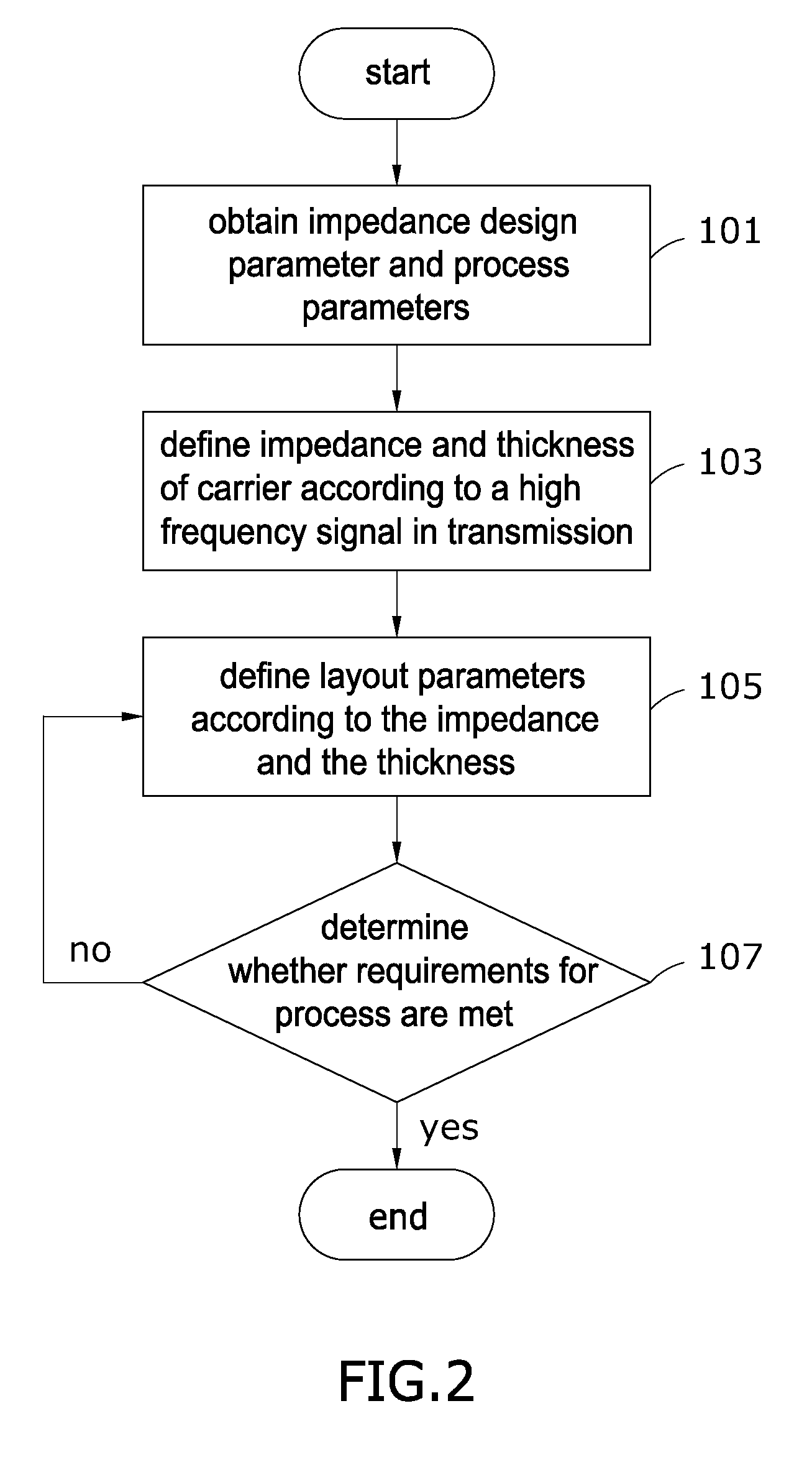
The foregoing signal transmission structure for transmitting a high speed signal to the carrier is likely to generate noise when coupled to another signals or transmit in a discontinuous structure, and thus the prior art is focused mostly on reduction of the harmonic of operation frequency.
Nonetheless, a low-pass filter cannot operate without greatly increasing the area of a chip working and affect the requirement of signal quality in conjunction with the low-pass filter.
More badly, given a variable process, intractability and inflexibility dog a delay unit in terms of delay time, for example.
Hence, the pre

Method used


Image

  • Carrier for transmitting high frequency signal and carrier layout method thereof
  • Carrier for transmitting high frequency signal and carrier layout method thereof
  • Carrier for transmitting high frequency signal and carrier layout method thereof

Examples


first embodiment

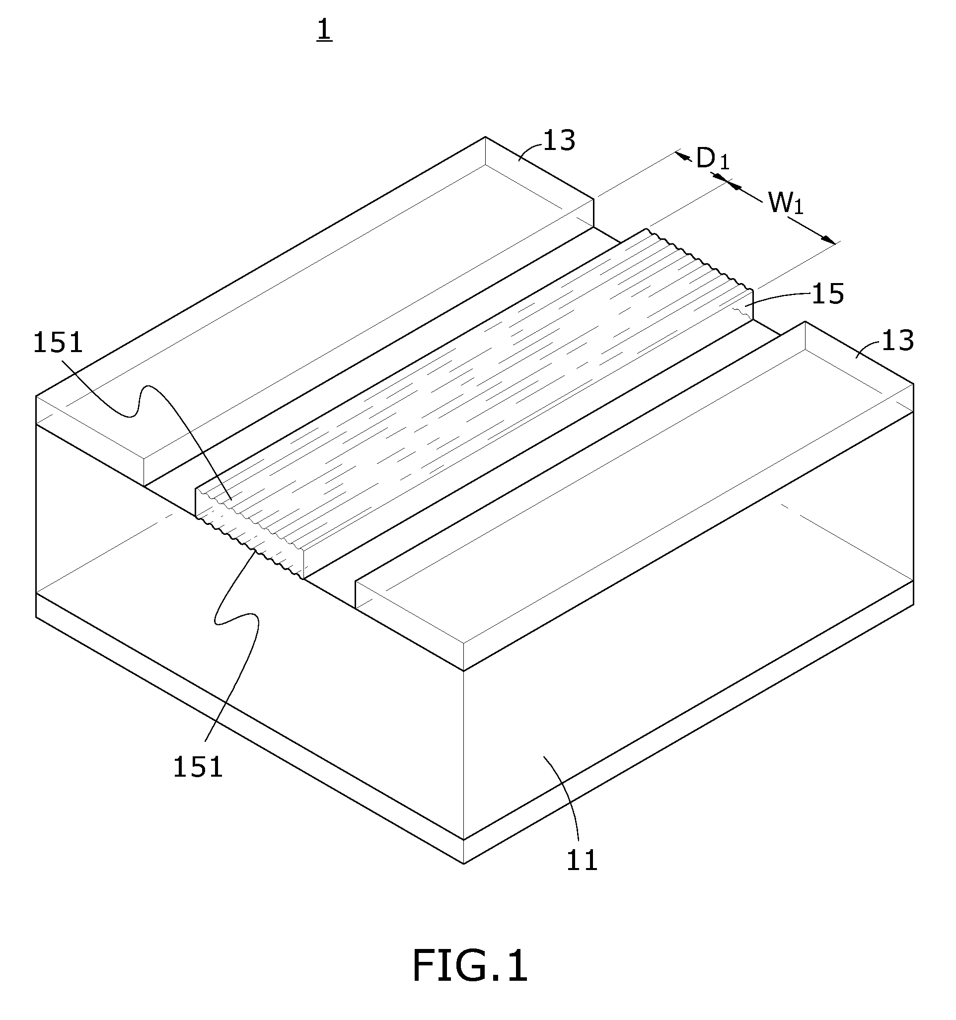
[0025]It should be noted that, in the first embodiment and the other embodiments, the carrier 1 is a circuit board, a bus line, and a flexible circuit board for use with communication products. The flexible circuit board is a flexible printed circuit board (flexible PCB), a flex-rigid PCB, or an equivalent circuit board.

[0026]The substrate 11 is a substrate with-high loss tangent (tan δ), such as an epoxy glass (FR4) substrate, or any other substrates with high loss tangent.

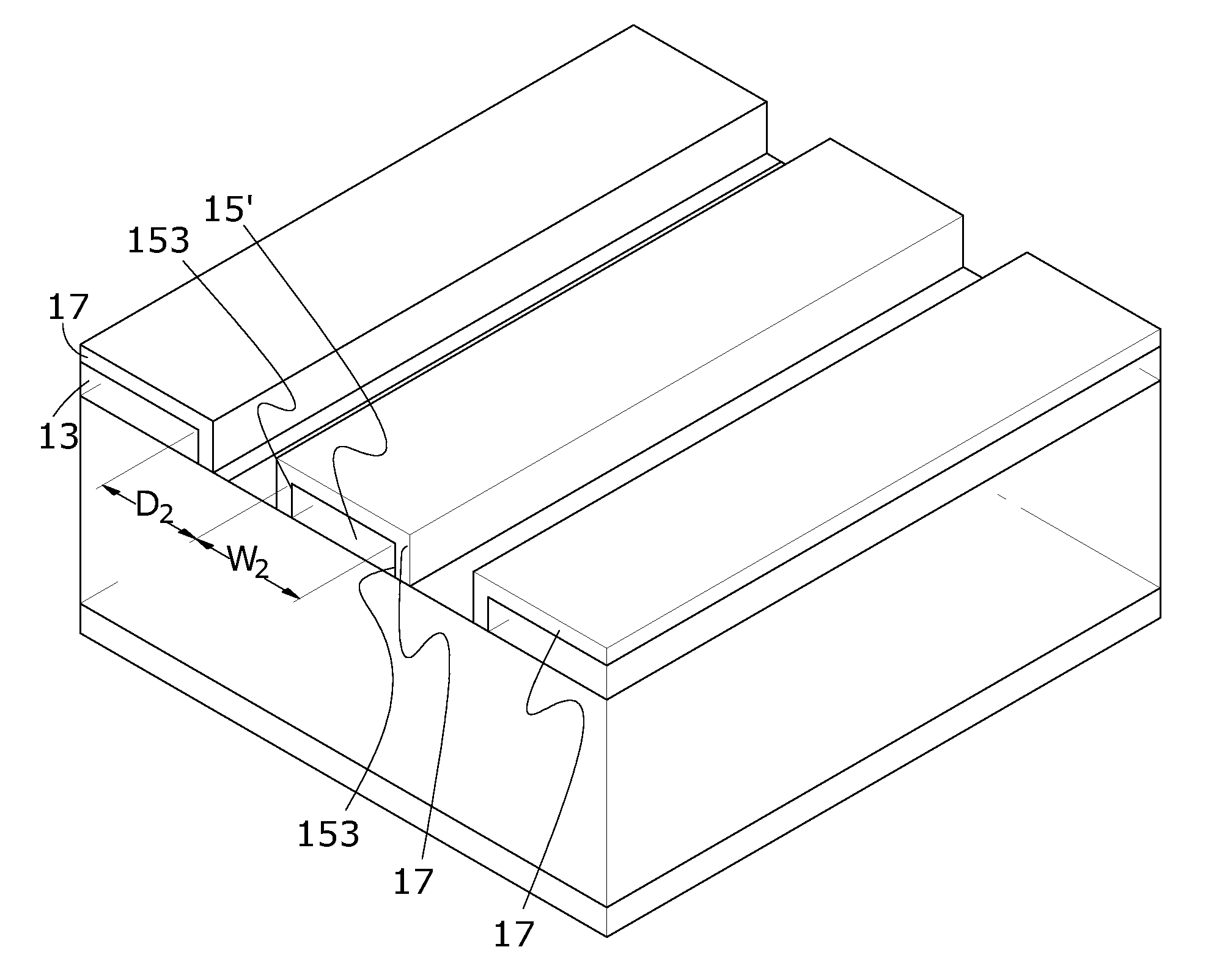
[0027]The reference planes 13 are formed on the substrate 11 and are power planes, ground planes, or other planes. In the first embodiment, the signal transmission structure comprises the reference planes 13 and the conducting wires 15. However, persons skilled in the art understand that the signal transmission structure is not limited to one described in the first embodiment.

[0028]The conducting wires 15 are formed on the substrate 11 and formed with roughness portions 151, and are of width W1. In the first embo...

second embodiment

[0046]Referring to FIG. 4, which is a schematic view of a layout in FIG. 3, the conducting wires 15′ have trace width denoted by width W2 and spacing denoted by distance D2, and a plurality of through holes 19 are formed in the reference planes 13. However, persons skilled in the art understand the positions of the through holes 19 are not limited by the

[0047]Of course, the present invention is always open to variation. For instance, a combination of at least one of the layout parameters can be provided. Referring to FIG. 5, the conducting layer 17 covers conducting wires 15″, the reference planes 13, and the substrate 11 in an indiscrete manner. Also, the drawing shows the following: the substrate 11 is of height H; there is distance D3 between the reference planes 13 and the conducting wires 15″; the conducting wires 15″ are of thickness T and are trapezoid-shaped, as the upper side and the lower side of the conducting wires 15″ are of width W3 and width W4, respectively, wherein ...


PUM


Abstract

A carrier for transmitting a high frequency signal and a carrier layout method thereof are provided. The carrier includes a substrate, conducting wires and reference planes both formed on the substrate. The carrier layout method includes defining impedance and thickness of the carrier according to the high frequency signal and defining layout parameters according to the impedance and the thickness. The layout parameters include a conducting layer formed on the conducting wires, a coplanar waveguide formed between the reference planes and the conducting wires, roughness portions formed on the conducting wires, recessed portions formed on the conducting wires, and the substrate being a high loss tangent substrate. The layout is performed according to the layout parameters defined thereabove, so as to increase loss of the high frequency signal in transmission.

Description

CROSS-REFERENCE TO RELATED APPLICATIONS[0001]This non-provisional application claims priority under 35 U.S.C. §119(a) on Patent Application No(s). 097149836 filed in Taiwan, R.O.C. on Dec. 19, 2008, the entire contents of which are hereby incorporated by reference.FIELD OF THE INVENTION[0002]The present invention relates to signal transmission, and more particularly, to a carrier for transmitting a high frequency signal and a carrier layout method thereof.BACKGROUND OF THE INVENTION[0003]Data transfer rate between communication products is ever-increasing. To ensure that transmission of a high frequency signal by a carrier is of high quality, the carrier, such as a print circuit board, or a cable such as flexible print circuit board / flat flexible cable (FPC / FFC), and Flex-rigid PCB, must have specified structure such as microstrip line, stripline and coplanar waveguide . . . etc so as for an electronic signal to be transmitted between conducting wires and to assure matching of chara...

Claims


Application Information

Patent Timeline
IPC IPC(8): H01P3/08
CPCH01P3/003H01P11/003H05K1/0219H05K1/0242H05K2203/0307H05K3/244H05K3/382H05K2201/0715H05K2201/09236H05K1/025H01P1/203H01P1/227H05K1/0216H05K1/0237
Inventor YANG, CHIH-MINGHUANG, CHIEN-HAOTSAI, CHAO-NANHSIEH, CHING-FENGCHANG, CHIN-CHINGTSAI, CHUN-HSIUNGCHANG, PI-CHIHUANG, CHIH-WEI
Owner ASKEY COMP
Why Eureka
Try Eureka