Electrostatic discharge protective circuit having rise time detector and discharge sustaining circuitry

a protection circuit and electrostatic discharge technology, applied in the field of integrated circuits, can solve the problems of packaged integrated circuits being exposed to electrostatic charges, integrated circuits are susceptible to damage, and excessive electrical charges, and achieve the effect of increasing the stability of the esd protection circui

Active Publication Date: 2010-06-24
SANDISK TECH LLC
View PDF21 Cites 31 Cited by
  • Summary
  • Abstract
  • Description
  • Claims
  • Application Information

AI Technical Summary

Benefits of technology

[0012]An electrostatic discharge (ESD) protection circuit embodiment includes a first RC circuit associated with a first RC time constant. The circuit being connected to a first voltage rail to produce a first RC based triggering signal in response to an electrostatic discharge on the first rail. The ESD circuit also has a shunt configured to shunt ESD energy away from a protected circuit when activated. The embodiment also includes a second RC circuit to produce a second RC based activation signal. The second circuit coupled with the first RC circuit and the shunt circuitry and configured so that the circuit operates as a duration control circuit. Accordingly, it produces the activation signal in response to the triggering signal received from the first RC circuit. The activation signal activates the shunt circuit and maintains the shunt in an active state for an extended period of time associated with a second RC time constant of the second RC circuit. The second RC time constant is substantially longer than the first RC time constant. Some associated embodiments can achieve the desired performance without added latch circuitry.
[0017]In another embodiment, an IC device includes an input pin coupled with an internal circuit and an electrostatic discharge (ESD) circuit arranged to protect the internal circuit from excessive voltage spikes applied at the input pin. Such an ESD circuit comprises trigger circuitry and shunt circuitry. The trigger having a small RC time constant. The trigger configured to activate the shunt when an input signal exceeds a threshold value for slew rate. The shunt circuitry, when activated by the trigger redirects the input signal away from the internal circuitry. The ESD circuit further includes shunt duration circuitry configured to maintain the shunt in an activated condition beyond that specified by the RC time constant of the trigger circuitry thereby enabling the shunt circuitry to discharge an ESD event to an extent that it will not damage the internal circuitry.
[0018]In another embodiment the shunt duration circuitry includes latch circuitry that increases the stability of the ESD protection circuit in noisy environment and other voltage variations inherent in the ordinary operation of the protected circuitry. An embodiment can be configured so that the trigger activates the shunt when an electrostatic discharge event occurs at the power input pin but does not activate the shunt when the input signal is an intended input signal. IC device embodiments can be configured so that the shunt duration circuitry maintains the shunt in an activated condition until the voltage from the input signal is less than about 1.5 times the normal operating voltage of the internal circuitry.

Problems solved by technology

Integrated circuits are susceptible to damage from application of excessive electrical charge, such as those generated during electrostatic discharge (ESD) events.
In other cases, a packaged integrated circuit may be exposed to electrostatic charges when a person inadvertently touches the exposed pins on the circuit package, or when the package becomes electro-statically charged due to movement of the package across an electrically-conductive surface.
The electrical pulse transferred to an integrated circuit (IC) during an ESD event can inflict significant damage to sensitive components of the integrated circuit.
For example, transistors and other electrical devices on an integrated circuit may be damaged when an excessive amount of charge is transferred between one or more pins of the integrated circuit and another conducting object over a short time period, usually between tens and hundreds of nanoseconds.
So far these devices have been unable to fully solve existing and constantly evolving ESD problems.
Existing devices can be overly sensitive to initial normal power up conditions, mistakenly redirecting normal power up voltages to ground and generating unnecessary and undesirable voltage spiking in the IC.
Such “false positives” are highly undesirable and interfere with the normal function of the internal circuitry.
Known circuits of this type frequently do not stay active long enough to sufficiently discharge the ESD event.
Although such snapback devices are often used within ESD protection devices, they are not without disadvantages.
For example, it is hard to predict / control the behavior of actual snapback devices fabricated in silicon, since the behavior of their parasitic BJTs cannot be accurately simulated (due to the fact that snapback devices operate in a region (the snapback region) which is largely unmodeled) and their parameters can be difficult to control in an actual implementation.
This lack of predictability can lead to inferior ESD protection performance or over-designed networks or both.
Consequently, such ESD protection schemes can consume relatively large amounts of silicon area and can affect the stand-by current budgets of the chips they are used in.
However, active network circuits suffer from some serious limitations and can fail provide adequate ESD protection in all cases.
As with snapback devices, the behavior of active network circuitry is also hard to control over process variations.
In some cases, the active network circuits may fail to protect the internal circuitry from a true ESD event due to process variations that affect the ESD protection circuitry operating parameters.
Such failure may allow a potentially damaging electrostatic charge to be supplied to the internal circuitry of an integrated circuit.
Unfortunately, such a process is time consuming and costly.
In addition, the ESD circuits resulting from such a process cannot be reused for other chips (e.g., with different sizes and / or ESD requirements).
Although such circuits are sensitive to ESD events they suffer from an inability to sufficiently discharge ESD events and so do not provide the desired level of ESD protection.
ESD protection circuits employing longer RC time constants feature improved discharge capability, but suffer from the inability to effectively distinguish ordinary operational and systemic noise from actual ESD events thereby seriously limiting their usefulness.
However, these circuits are large, complicated, and require programming time that can substantially increase the cost.

Method used


Image

  • Electrostatic discharge protective circuit having rise time detector and discharge sustaining circuitry
  • Electrostatic discharge protective circuit having rise time detector and discharge sustaining circuitry
  • Electrostatic discharge protective circuit having rise time detector and discharge sustaining circuitry

Examples


Embodiment Construction

[0030]The present invention has been particularly shown and described with respect to certain embodiments and specific features thereof. The embodiments set forth herein below are to be taken as illustrative rather than limiting. It should be readily apparent to those of ordinary skill in the art that various changes and modifications in form and detail may be made without departing from the spirit and scope of the invention.

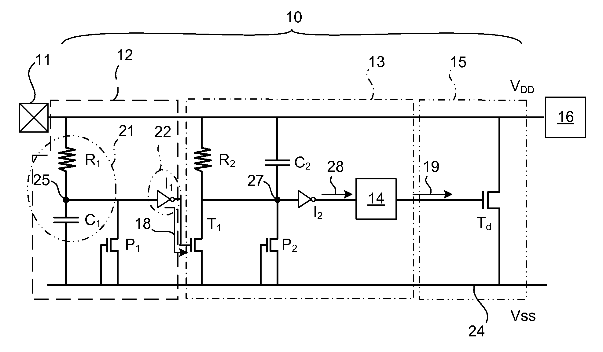
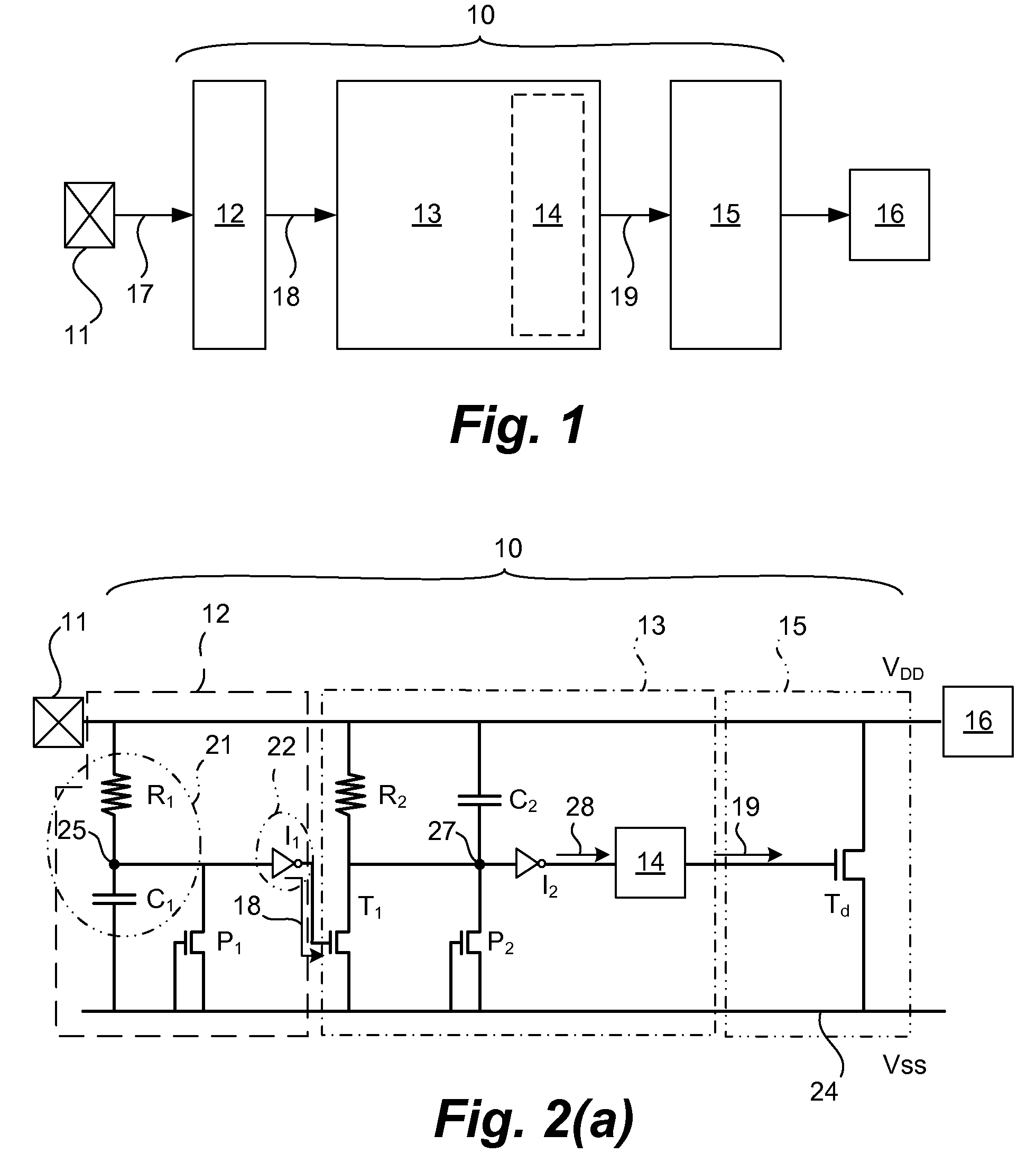
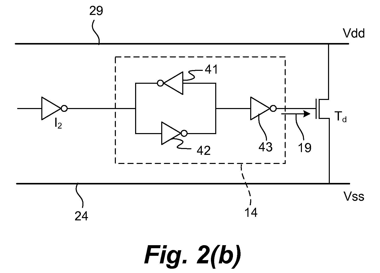
[0031]The following detailed description describes various embodiments of an ESD protection device and methods for its use. In particular, embodiments of the present invention are configured to rapidly respond to ESD events having a very high slew rate and maintain circuit protection for an extended period of time enabling very high voltages to be sufficiently redirected away from the protected circuitry.

[0032]Although the resistance of an ESD event depends much on the precise circuitry being protected, the terms “excessive voltage”, “excessive voltage”, “ESD en...


PUM


Abstract

Methods and devices of the invention include an electrostatic discharge (ESD) protection circuit. This circuit includes rise time dependent activation circuitry capable of detecting a slew rate of an input signal and capable of determining whether the slew rate of the input signal is greater than a threshold value. For an ESD event said activation circuitry generates a trigger signal. Additionally, the activation circuitry is coupled with the ESD dissipation duration control circuitry which is further coupled with an ESD dissipation circuit. This arrangement enabling the duration control circuit to be activated by the trigger signal which responds by producing an activation signal that activates the ESD dissipation circuitry and that controls the length of time the dissipation circuit remains active. The ESD dissipation circuitry includes a shunt that redirects the ESD energy away from the protected internal circuit. The ESD dissipation duration circuitry further configured to maintain shunting of the energy for a period of time sufficient to discharge of the ESD energy without damaging the protected circuitry.

Description

TECHNICAL FIELD[0001]This invention relates to integrated circuits and, more particularly, to circuitry for protecting integrated circuit components from damage caused by high slew rate, overvoltage and / or excessive current conditions, such as those caused by electrostatic discharge.BACKGROUND[0002]The following descriptions and examples are given as background only.[0003]Integrated circuits are susceptible to damage from application of excessive electrical charge, such as those generated during electrostatic discharge (ESD) events. For example, integrated circuits (ICs) may be exposed to electrostatic charges during manufacturing of the integrated circuit (wafer level), handling of the integrated circuit after packaging and / or handling of a printed circuit board after assembly. In some cases, an integrated circuit may be exposed to the charges that arise from the use of plasma etching techniques or other fabrication processes that produce charged particles. In other cases, a packag...

Claims


Application Information

Patent Timeline
Patent Type & Authority Applications(United States)
IPC IPC(8): H02H9/04
CPCH01L27/0266H03K19/00315H03K17/08122
Inventor HONG, RICHARD J.K.
Owner SANDISK TECH LLC
Why Eureka
Try Eureka