

Material for organic photoelectric device, and organic photoelectric device including the same
- Summary
- Abstract
- Description
- Claims
- Application Information
AI Technical Summary
Benefits of technology
Problems solved by technology
Method used
Image

Examples
example 1-1
Synthesis of Organic Compound (5)
[0086]A bipolar organic compound (5) as a material for an organic photoelectric device was synthesized as shown in the following Reaction Scheme 1.
[0087]Step 1: Synthesis of First Intermediate (A)
[0088]50.8 g (304 mmol) of carbazole, 71.6 g (304 mmol) of 1,4-dibromobenzene, 3.76 g (38 mmol) of cuprous chloride, and 83.9 g (607 mmol) of potassium carbonate were suspended in 322 ml of dimethylsulfoxide, and refluxed under a nitrogen atmosphere for 8 hours while heating. The refluxed reaction fluid was cooled to room temperature and recrystallized with methanol.
[0089]The precipitated crystals were separated by filtration and the obtained residue was purified by silica gel column chromatography, providing 59.9 g of the first crystalline intermediate (A) (yield 61.3%).
[0090]Step 2: Synthesis of Second Intermediate (B)
[0091]37.8 g (117 mmol) of the first intermediate product (A) was dissolved in 378 ml of tetrahydrofuran, then 100.5 ml (161 mmol) of n-buty...
example 1-2
Synthesis of Organic Compound (10)
[0096]A bipolar organic compound (10) having the above Formula 13 as a material for an organic photoelectric device was synthesized as shown in the following Reaction Scheme 2.
[0097]Step 1; Synthesis of First Intermediate (C)
[0098]40.4 g (241 mmol) of carbazole, 38.0 g (121 mmol) of 1,3,5-tribromobenzene, 2.99 g (30 mmol) of cuprous chloride, and 66.7 g (483 mmol) of potassium carbonate were suspended in 171 ml of dimethyl sulfoxide, and heated and refluxed under a nitrogen atmosphere for 8 hours.
[0099]The refluxed reaction fluid was cooled to room temperature and recrystallized with methanol. The precipitated crystals were separated by filtration and the obtained residue was purified by silica gel column chromatography, providing 59.9 g of the first crystalline intermediate (C) (yield 62.4%).
[0100]Step 2: Synthesis of Second Intermediate (D)
[0101]35.0 g (72 mmol) of the first intermediate (C) was dissolved in 350 ml of tetrahydrofuran, then 61.5 ml...
example 2-1
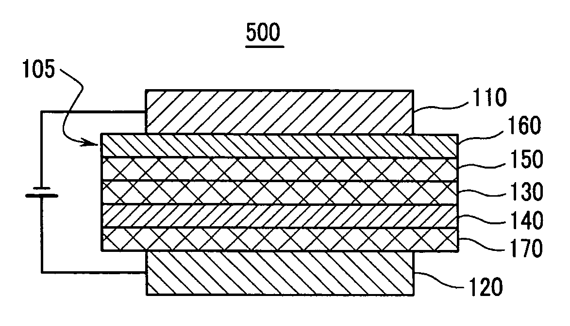
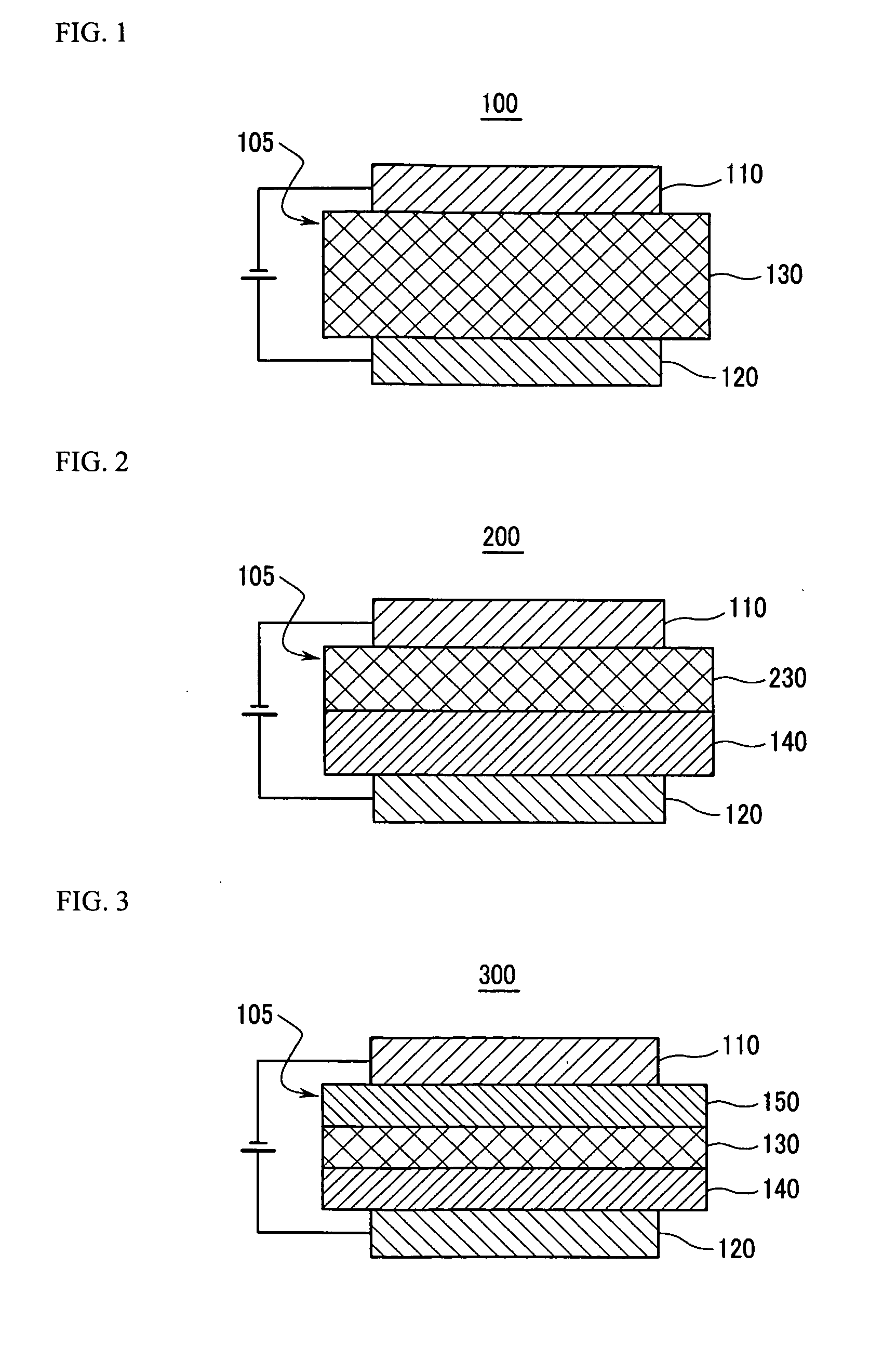
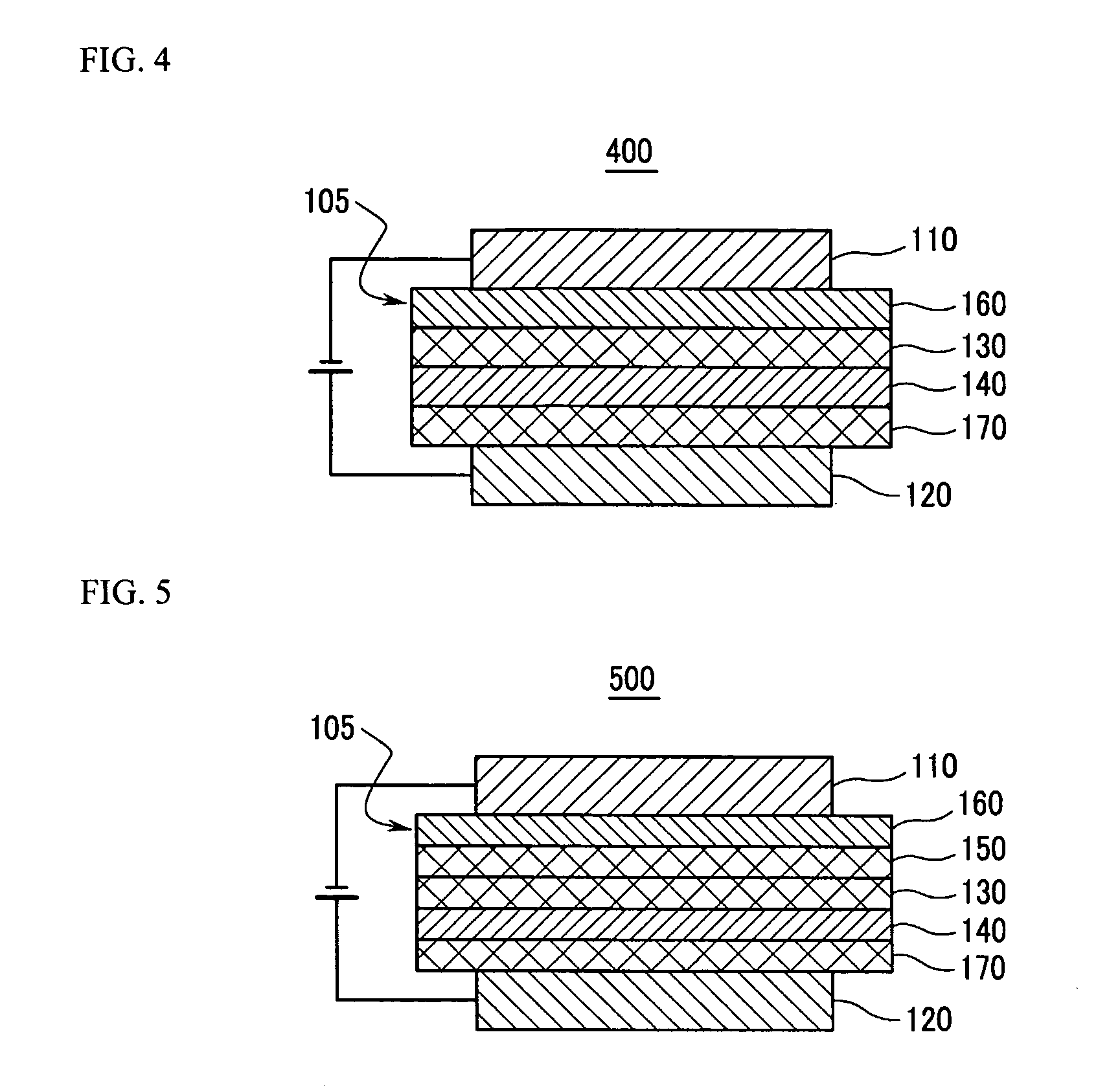
[0109]The organic compound (5) prepared from Example 1-1 was used as a host, and Ir(piq)2(acac) was used as a dopant to provide an organic photoelectric device.
[0110]ITO was provided in a thickness of 1000 Å for an anode, and aluminum (Al) was provided in a thickness of 1000 Å for a cathode.
[0111]The method of manufacturing an organic photoelectric device may be described in detail as follows: cutting an ITO glass substrate having a sheet resistance value of 15 Ψ / cm2 into a size of 50 mm×50 mm×0.7 mm for a cathode; ultrasonic wave cleaning the same in acetone, isopropyl alcohol, and pure water for 15 minutes, respectively; and UV ozone cleaning for 30 minutes.
[0112]N,N′-di(1-naphthyl)-N,N′-diphenylbenzidine (NPD) was deposited on the upper surface of the substrate under the conditions of a vacuum degree of 650×10−7 Pa and a deposition speed of 0.1 to 0.3 nm / s to provide a 300 Å-thick hole transport layer (HTL).
[0113]Subsequently, under the same vacuum deposition conditions, the orga...
PUM
| Property | Measurement | Unit |
|---|---|---|
| Temperature | aaaaa | aaaaa |
| Temperature | aaaaa | aaaaa |
| Temperature | aaaaa | aaaaa |
Abstract
Description
Claims
Application Information