
Assembly of nanoscaled field effect transistors

a field effect transistor and nano-scale technology, applied in the direction of transistors, electrical devices, nanotechnology, etc., can solve the problems of inability to fabricate efets,

Inactive Publication Date: 2010-07-15
QUNANO
View PDF25 Cites 77 Cited by
  • Summary
  • Abstract
  • Description
  • Claims
  • Application Information

AI Technical Summary

Benefits of technology

[0008]The nanowire technology according to the present invention allows for flexibility in the design and the fabrication of the transistors on the same chip. Nanowires with different diameters may be grown in the same growth run utilizing different sizes of the metal catalysts. This allows for a integration of transistors with different threshold voltages. Yet a further advantage is the possibility to tailor the bandstructure along the transport channel using segments of different band gap and or doping levels. This allows for a reduction in both the source-to-gate and gate-to-drain access resistance. These segments may be incorporated directly during the growth, which is not possible in the planar technologies. In particular, this may improve the critical high-frequency performance of the EFETs.
[0009]This invention describes various ways to control the threshold voltage in wrap-gated nanowire transistors via nanowire design. The threshold voltage may be controlled by the diameter of the nanowire, the doping level in the nanowire, the introduction of heterostructure segments in the nanowire, the addition of doped layers surrounding the nanowire, tailoring of the workfunction in the gate stack, or by strain-engineering of the channel. The present invention facilitates the possibility to combine transistors with different threshold voltages and in particular the combination of enhancement- and depletion-mode transistors.

Problems solved by technology

Obviously the prior art methods have drawbacks with regards to being able to fabricate EFETs and combinations of EFETs and DFETs in small dimensions.
These segments may be incorporated directly during the growth, which is not possible in the planar technologies.

Method used


Image

  • Assembly of nanoscaled field effect transistors
  • Assembly of nanoscaled field effect transistors
  • Assembly of nanoscaled field effect transistors

Examples


Embodiment Construction

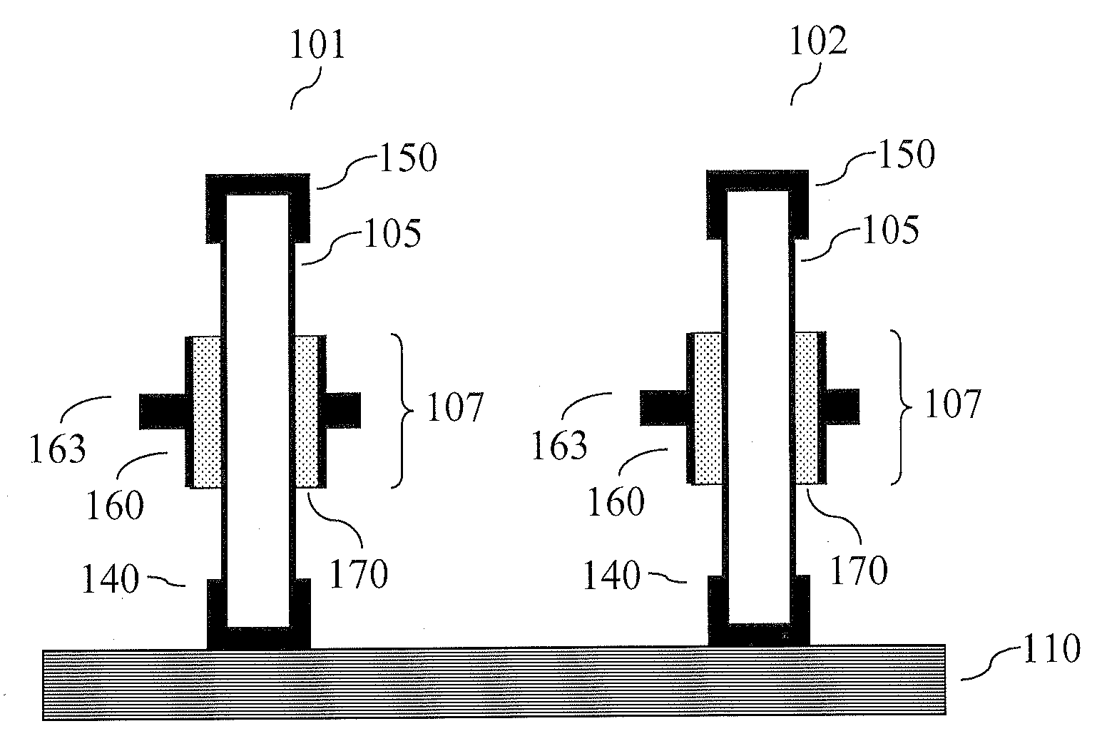
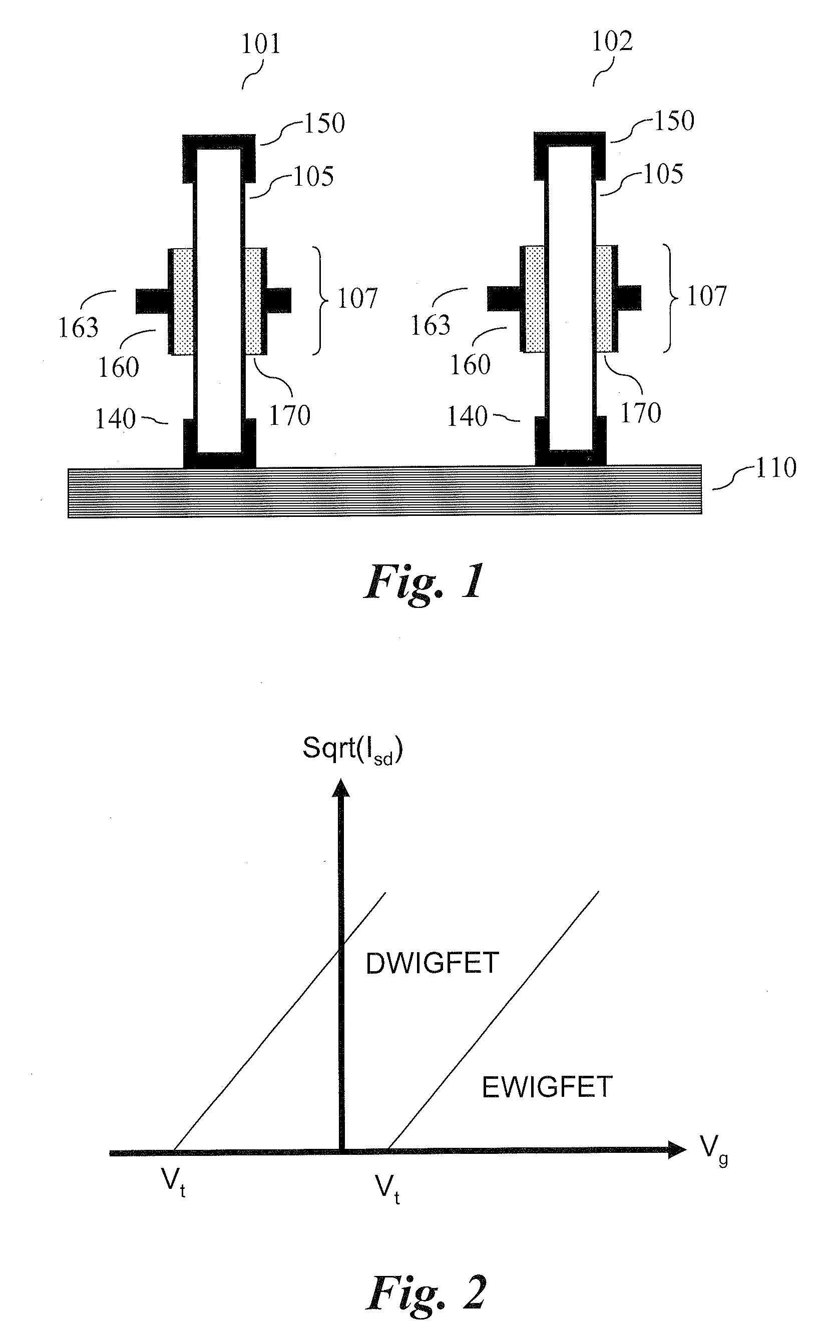
[0025]A semiconductor device according to the invention is schematically illustrated in FIG. 1. The device comprises an assembly of at least two wrap gate field effect transistors (WIGFET) 101, 102. Each of the transistors comprises a nanowire 105 typically of a III / V semiconductor, as a channel. The nanowires 105 are massive as compared to nanotubes, which are hollow cylinders. Although massive, the nanowires may comprise on more segments of different material compositions. The nanowires 105 has been grown on a substrate 110. In one end of the nanowires source contacts 140 are provided and in the opposite end drain contacts 150. Between the source contacts 140 and drain contacts 150 are gate contacts 160 arranged. The gate contacts 160 surrounds, or wraps, the respective nanowire 105, and covers a portion, the gate portion 107 of the respective nanowire. The substrate 110 may form the source contact 140. Alternatively, a dedicated source contact 140 in the form of a patterned layer...


PUM


Abstract

The present invention relates to vertical nanowire transistors with a wrap-gated geometry. The threshold voltage of the vertical nanowire transistors is controlled by the diameter of the nanowire, the doping of the nanowire, the introduction of segments of heterostructures in the nanowire, the doping in shell-structures surrounding the nanowire, tailoring the work function of the gate stack, by strain engineering, by control of the dielectrica or the choice of nanowire material. Transistors with varying threshold voltages are provided on the same substrate, which enables the design of advanced circuits utilizing the shifts in the threshold voltages, similar to the directly coupled field logic.

Description

TECHNICAL FIELD[0001]The present invention relates to nanoscaled field effect transistors. In particular the invention relates to a device comprising an assembly of nanowire wrap-gated field effect transistors.BACKGROUND[0002]The transistor is the fundamental building block for electronic circuit design. Performance metrics, like speed, power consumption and the number of transistors used are directly related to the choice of transistor technology that is used for the implementation. The selected technology may hence strongly influence the circuit performance.[0003]The main factors that define a field-effect transistor (FET) are the type of carriers used (n or p) and the threshold voltage. The type of carriers determines the response of an input voltage to the gate on the output current at the drain terminal. For a n-type device the on-current is increased as the gate voltage is increased, while for a p-type device the on-current is decreased as the gate voltage is increased. The ty...

Claims


Application Information

Patent Timeline
IPC IPC(8): H01L27/088H01L21/36
CPCB82Y10/00H01L27/0883H01L29/0665H01L29/0673H01L29/7828H01L29/068H01L29/20H01L29/775H01L29/0676H01L21/02603
Inventor WERNERSSON, LARS-ERIKLIND, ERIKBRYLLERT, TOMASOHLSSON, JONASLOWGREN, TRULSSAMUELSON, LARSTHELANDER, CLAES
Owner QUNANO
Learn More