Solar photovoltaic structure comprising quantized interaction sensitive nanocells

a nano-cell and photovoltaic technology, applied in the field of solar photovoltaic structure comprising quantized interaction sensitive nano-cells, can solve the problems of inability to meet the sensitivity level and the inability of u.s. pat. no. 4,445,050, and achieve the effects of increasing efficiency, high efficiency, and increasing solar cell efficiency

Inactive Publication Date: 2010-08-05
THE GERALD C HUTH & BARBRO M DROTT HUTH TRUST +3
View PDF18 Cites 6 Cited by
  • Summary
  • Abstract
  • Description
  • Claims
  • Application Information

AI Technical Summary

Benefits of technology

[0010]An array of the above described nanocells uniquely provides a solar photovoltaic device structure capable of detecting individual photons (or light quanta) and converting these single-photon signals into electrical energy. As noted above, because separation of electrical charge is maintained within each nanocell, many millions of individual “rectenna” sites may be obtained over a square inch of area of the surface of the device. Simple calculation shows that even at solar fluence the probability of two photons being incident on a single optical antenna site of this large number of individual cells is negligible. The nanostructure thus precludes out-of-phase signal cancellation and increases efficiency beyond the confines of expected classical solar cell models.
[0011]It is shown in the present invention that each nanocell provides a site capable of detecting and converting single-photons into electrical energy. It follows from a simple calculation showing that even at solar fluence (˜10>21 photon/m2/sec) the probability of two photons being incident on a single light interacting antenna nanocell of this large number (density ˜10>14 nanocells/m2) of individual cells is negligible. The combination of solar fluence, the density of nanocells and the wavelength

Problems solved by technology

This level of sensitivity has not been matched photonic device technology that is only able to single photons by applying use of cryogenic cooling to liquid helium temperatures or using high levels of electronic amplification (“photomultip

Method used


Image

  • Solar photovoltaic structure comprising quantized interaction sensitive nanocells
  • Solar photovoltaic structure comprising quantized interaction sensitive nanocells
  • Solar photovoltaic structure comprising quantized interaction sensitive nanocells

Examples


Embodiment Construction

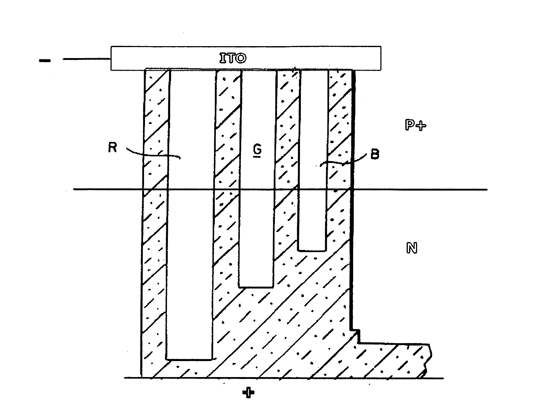
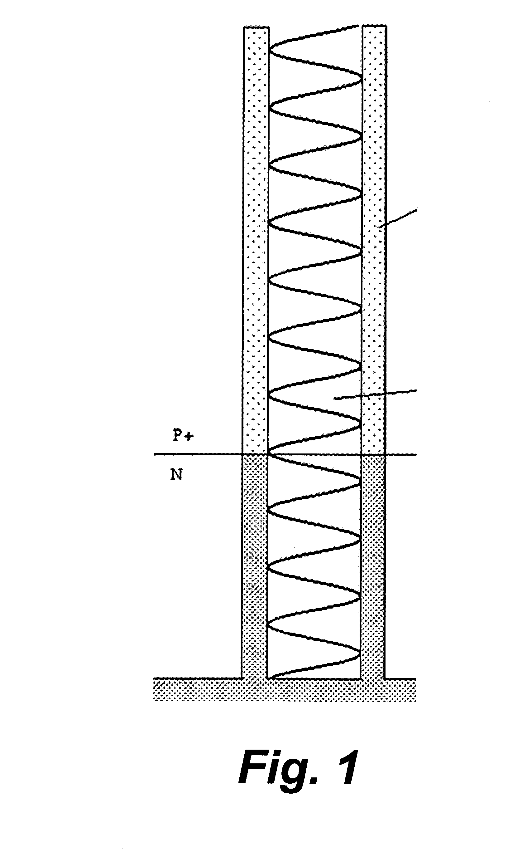
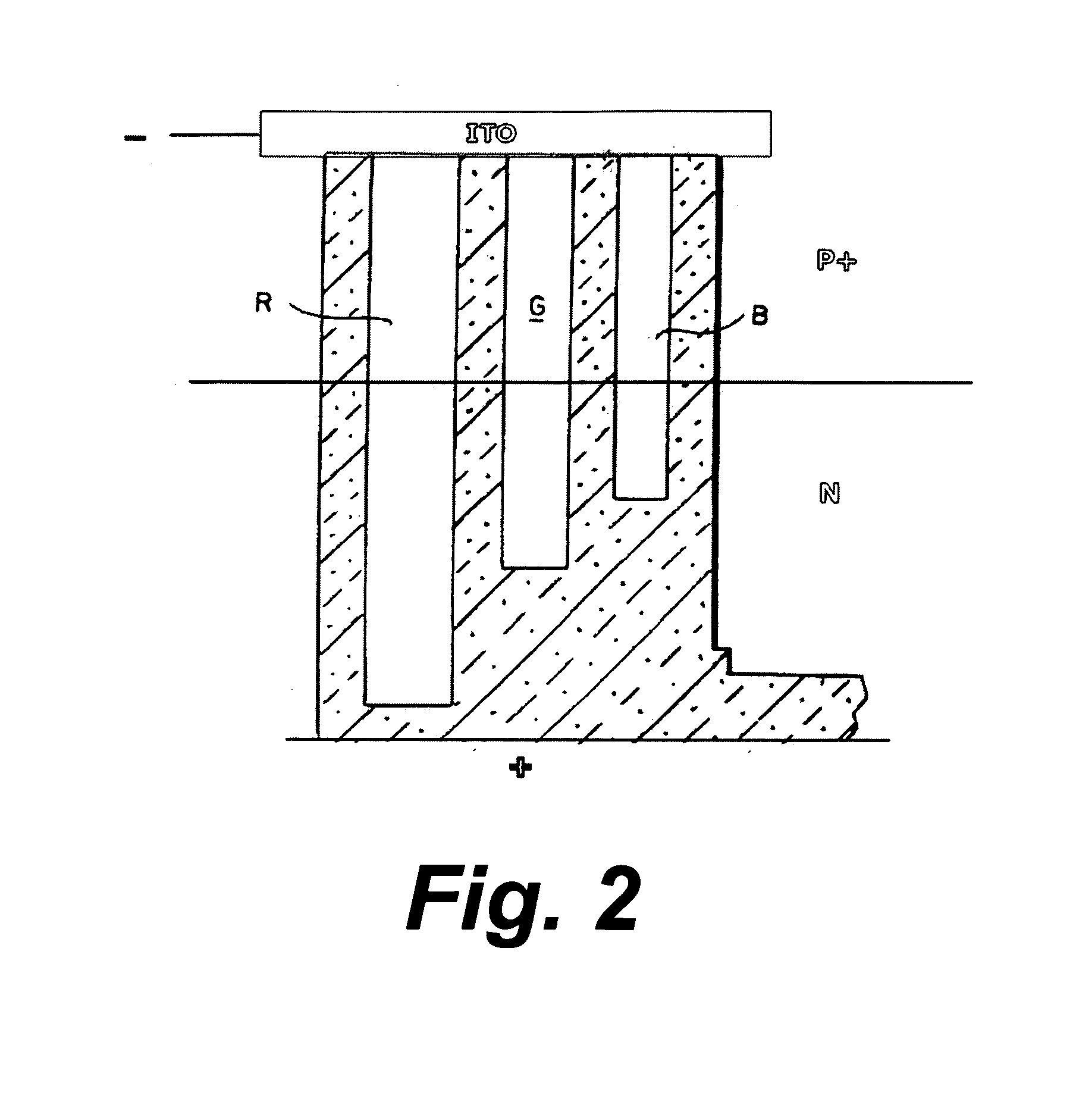
[0024]The present invention relates to a novel light to electrical power converting structure comprised of individual “nanocells”, each being defined as an energy converting structure comprising (1) A sub-micron dimensioned, “antenna” light interaction space or spaces wherein light is absorbed as the wave of classical physics, with this space or spaces being immediately adjacent to a fixed dimension quantum confined electron space or spaces (“EQC”) that forms the absorbing mass, and, (2) wherein each nanocell provides for separation of electrical charge (using, for example, a pn or Schottky barrier junction) contained within each nanocell. The single or fundamental nanocell can also be described as the basic “building block” of an overall solar cell array structure. In some embodiments of the present invention, each nanocell comprises a optical light wave-accepting region fabricated, for example, as a cavity on the surface of a semiconductor, which is intimately and directly bounded...


PUM


Abstract

A light-to-electrical energy conversion device comprising a nano structure is formed on a surface of a semiconductor substrate. The nanostructure comprises an array of basic light antenna nanocells, with the individual antenna nanocells formed as “rectenna” structures. Light energy is absorbed within each independent antenna nanocell and converted to direct current. In one particular configuration, the structure of each basic nanocell comprises a cavity or cavities dimensioned to accept light as the wave of classical physics. These cavities function as quantum confinement sites for electrons that constitute an absorbing mass. The cavity dimensionality provides a determinative factor in wavelength discrimination of the nanocell structure.

Description

FIELD OF THE INVENTION[0001]This invention relates to devices for converting light power to electric power and electric power to light power. More particularly it relates to achieving high light conversion efficiency in solar photovoltaic devices, comprising an array of independent, uniquely defined, light detecting and rectifying nanocells.BACKGROUND OF THE INVENTION[0002]The photovoltaic solar cell was first developed over fifty years ago and used a pn junction diffused into silicon. In the intervening years, and after intensive research conducted around the world, the efficiency of such devices to convert light into electrical power has been only incrementally improved from that time. Efficiency values today are generally about 20-25% for highly optimized cells for space application and about 10% for commercially available terrestrial cells. Increasing the efficiency values of photovoltaic cells with resultant economic implications may be the single most critical energy research ...

Claims


Application Information

Patent Timeline
IPC IPC(8): H01L31/0352H01L31/00H01L31/18
CPCH01L31/0284H01L31/0352H01L31/068Y02E10/547H01L31/103H01L31/108H01L31/1804H01L31/07H01L31/035227Y02P70/50
Inventor HUTH, GERALD C.
Owner THE GERALD C HUTH & BARBRO M DROTT HUTH TRUST
Why Eureka
Try Eureka