

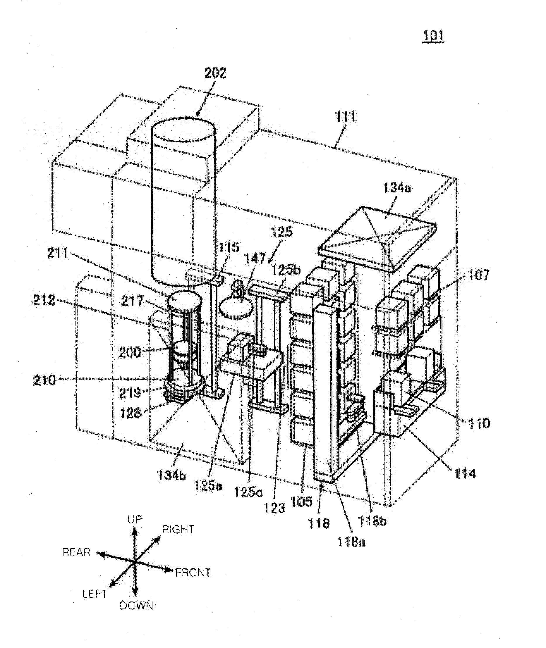
Semiconductor device manufacturing method and substrate processing apparatus
a technology of semiconductor devices and processing apparatus, which is applied in the direction of coatings, chemical vapor deposition coatings, metallic material coating processes, etc., can solve the problems of low-temperature processing and the possibility of impurity rediffusion
- Summary
- Abstract
- Description
- Claims
- Application Information
AI Technical Summary
Benefits of technology
Problems solved by technology
Method used
Image

Examples
first embodiment
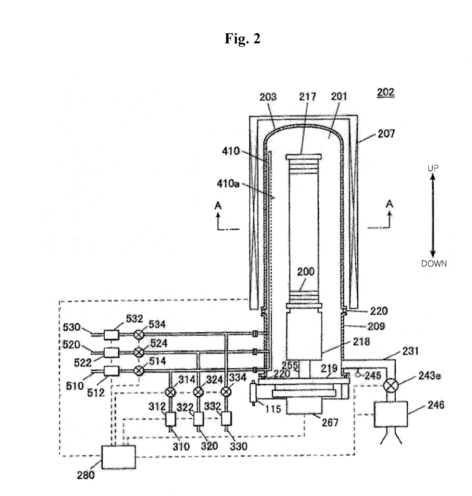
[0081]In the current embodiment, an explanation will be given on an example of forming a silicon oxide film on a substrate as an insulating film by using trichloro silane (SiCl4) as a silicon-containing gas, water (H2O) as an oxidizing gas, and ammonia (NH3) as a catalyst. NH3 is used as a catalyst because a nitrogen (N) atom of a NH3 molecule has a lone pair of electrons that attracts hydrogen (H). The degree of a force attracting hydrogen is expressed by an acid dissociation constant (pKa), and NH3 has a pKa of about 11. A large pKa means a strong hydrogen attracting force, and NH3 has such characteristics. FIG. 4 is a view illustrating a relationship between film-forming rate and film-forming temperature when a silicon film is formed using NH3 as a catalyst. In FIG. 4, the film-forming temperature means the inside temperature of the process chamber 201. As shown in FIG. 4, a film can be formed at a temperature of about 200° C. or lower, and the film-forming rate increases as the ...
second embodiment
[0110]It is necessary to prevent direct reaction between Cl (chlorine) and a catalyst for suppressing generation of particles. Generally, a substance having high acid dissociation constant tends to actively react with a substance including a group 17 element such as chlorine (Cl). Therefore, to suppress generation of particles, it is necessary to select a substance having low acid dissociation constant. For example, pyridine (C5H5N, pKa=5.7) is selected. In addition, SiCl4 (trichlorosilane) is used as a silicon-containing gas, and H2O (wafer) is used as an oxidizing gas. This exemplary case will now be described.
[0111]Furthermore, generation of particles can be reduced by setting the inside pressure of the process chamber 201 to a level lower than the vapor pressure of a byproduct generating after a film-forming process. However, if the inside pressure of the process chamber 201 is excessively low, the film-forming rate may be reduced to lower throughput. Therefore, preferably, a ca...
third embodiment
[0137]In the second embodiment, pyridine is used as a catalyst. However, since pyridine causes environmental pollution such as air pollution, the use of pyridine may be regulated by a law or be reported. A substance such as picoline has acid dissociation constant pKa similar to that of pyridine by less regulated by a law. Except for the used of a different kind of catalyst, the current embodiment is the same as the second embodiment, and thus a detailed description of the current embodiment will be omitted.
[0138]Another catalyst having acid dissociation constant pKa of about 5 to about 7 may be used. For example, catalysts such as pyridine, aminopyridine, picoline, piperazine, and lutidine can be used. Such substances have similar structures characterized by nitrogen (N) coupled to a heterocyclic ring. FIG. 19 illustrates structures of such substances.
[0139]Although substances such as pyrrolidine and piperidine are similar to the above-described substances, since they have acid diss...
PUM
| Property | Measurement | Unit |
|---|---|---|
| Temperature | aaaaa | aaaaa |
| Temperature | aaaaa | aaaaa |
| Electronegativity | aaaaa | aaaaa |
Abstract
Description
Claims
Application Information