P-channel silicon carbide mosfet

a silicon carbide and mosfet technology, applied in the direction of semiconductor devices, diodes, electrical apparatus, etc., can solve the problems of increasing device size, increasing cost, and aforementioned complementary igbt modules being currently unavailable on the market, and achieves low on-resistance characteristics, high avalanche breakdown tolerance, and high practical use value

Inactive Publication Date: 2010-09-09
FUJI ELECTRIC CO LTD
View PDF8 Cites 26 Cited by
  • Summary
  • Abstract
  • Description
  • Claims
  • Application Information

AI Technical Summary

Benefits of technology

[0014]According to the invention, it is possible to provide a p-channel silicon carbide MOSFET which has high ava...

Problems solved by technology

As a result, the configuration of the gate driving circuits is complicated causing an increase in device size and a resulting increase in cost.
The aforementioned complementary IGBT module is however currently unavailable on the market.
This is because breakdown tolerance of p-channel IGBT's is too low to endure practical use compared with that of n-channel IGBT's.
Accordingly, SiC p-channel MOSFET's of practical use as well as IGB...

Method used


Image

  • P-channel silicon carbide mosfet
  • P-channel silicon carbide mosfet
  • P-channel silicon carbide mosfet

Examples


embodiment 1

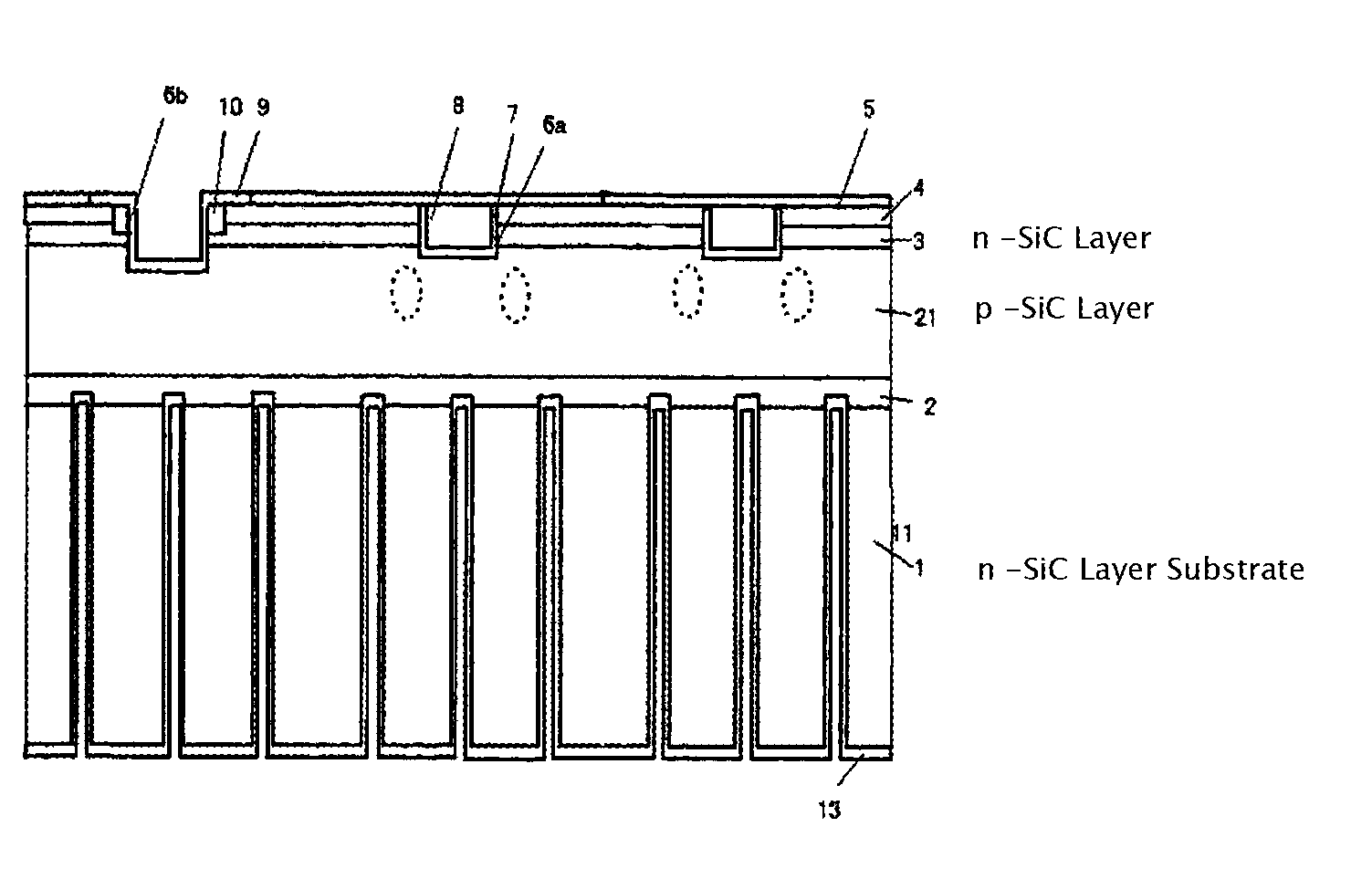
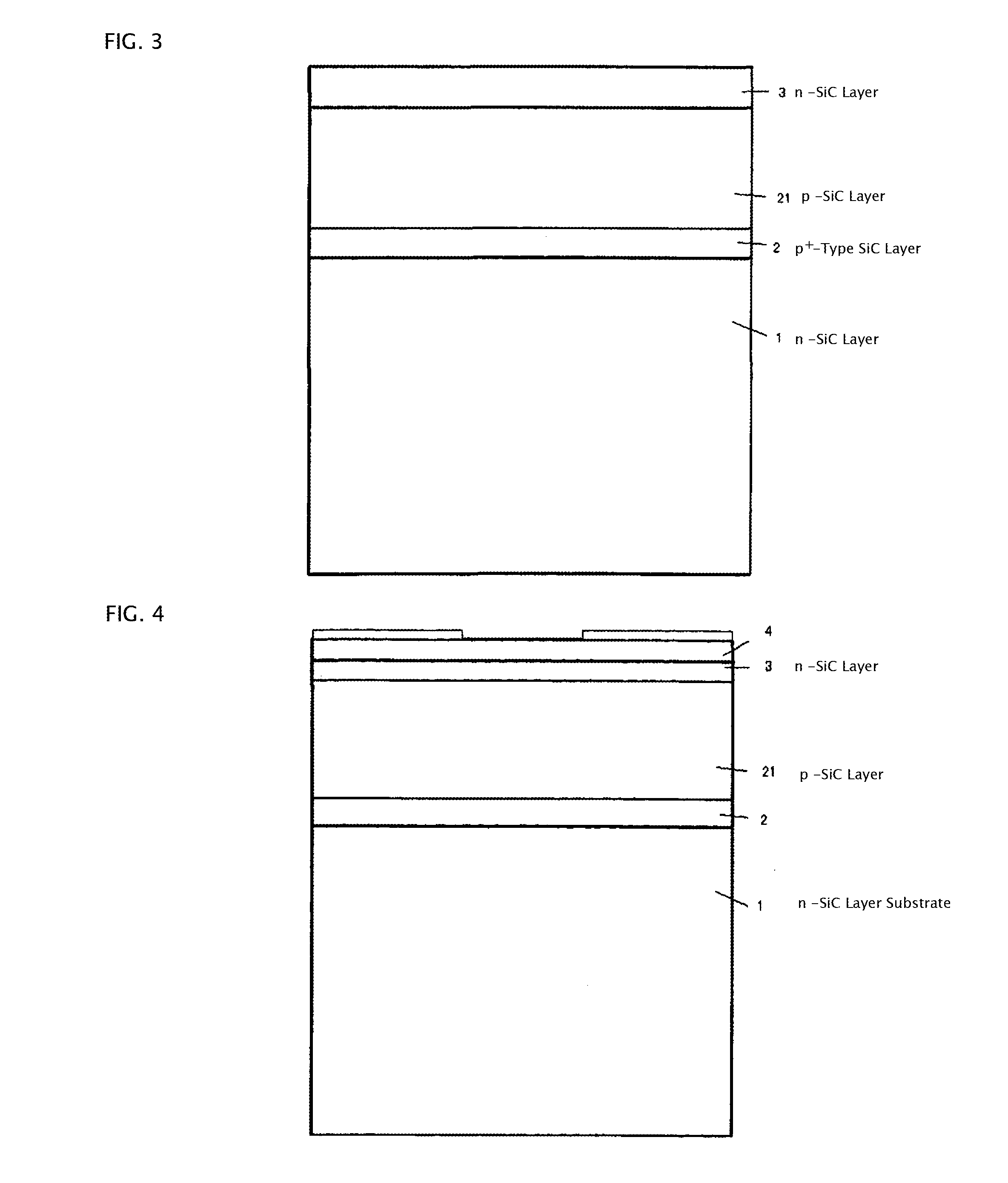
[0032]Embodiment 1 of the invention will be described below with reference to FIGS. 3 to 7. Incidentally, in Embodiment 1, a trench MOSFET with a withstand voltage of 1200 V is provided as a vertical SiC p-channel MOSFET. First, an n-type SiC semiconductor substrate 1 (referred to as n-SiC substrate in FIG. 3) with a thickness of 400 μm is prepared. In Embodiment 1, the substrate 1 is provided as a high-resistance SiC semiconductor substrate containing about 2×1014 cm3 of nitrogen as an impurity. However, in this embodiment, use of the high-resistance SiC semiconductor substrate is not essential, and a low-resistance SiC semiconductor substrate is also usable for a semiconductor substrate. A high impurity concentration p+-type SiC layer 2 containing about 1.0×1019 cm−3 of an impurity and a p-type base layer 21 (referred to as p-SiC layer 21 in FIG. 3) containing about 1.0×1016 cm−3 of an impurity (the semiconductor layers described hereinafter are all SiC layers if there is no parti...

embodiment 2

[0050]Embodiment 2 will be described on a trench MOSFET with a withstand voltage of 1200 V in the case where a p-type SiC substrate is used as an SiC substrate. Embodiment 2 is different from Embodiment 1 in the polarity and specific resistance (resistivity) of the SiC substrate. First, an aluminum-doped p-type SiC substrate was prepared. In this embodiment, a p-type SiC substrate containing an impurity concentration of about 2×1018 cm−3 was used. The specific resistance of the p-type SiC substrate was 7 Ωcm which was far lower than that of the n-type SiC substrate described in Embodiment 1. The element forming process after that was performed in the same manner as in Embodiment 1. The chip size was 3 mm square, the area of the active portion was 7.85 mm2, and the rating current was 10 A. On-resistance (RonA) exhibited a sufficiently low value of 2.56 mΩcm2. The initial element withstand voltage was 1258 V which exhibited sufficiently good characteristic of a 1200 V element. When I-...

embodiment 3

[0052]In a p-type SiC substrate with low resistance and low crystal defect density, it is however unnecessary to form deep third trenches in the other surface of the substrate in the aforementioned manner. In this case, an MOSFET having a layer structure composed of a p-type SiC semiconductor substrate 1, a p-type base layer 21 with a low impurity concentration formed on the p-type SiC semiconductor substrate 1, and an n-type base layer 3 formed on the p-type base layer 21 may be produced in the same manner as a usual MOSFET.

[0053]Embodiment 3 will be described on a trench MOSFET (FIG. 13) with a withstand voltage of 1200 V in the case where a low-resistance p-type SiC substrate is used as the SiC semiconductor substrate 1. Embodiment 3 is different from Embodiment 2 in that the specific resistance of the p-type SiC in Embodiment 3 is far lower. As a result, Embodiment 3 does not require the third trenches formed in the rear surface of the p-type SiC substrate in Embodiments 1 and 2...


PUM


Abstract

A second trench in each source electrode portion (Schottky diode portion) is formed to have a depth equal to or larger than the depth of a first trench in each gate electrode portion. The distance between the first and second trenches is set to be not longer than 10 μm. A source electrode is formed in the second trench and a Schottky junction is formed in the bottom portion of the second trench. In this manner, it is possible to provide a wide band gap semiconductor device which is small-sized, which has low on-resistance and low loss characteristic, in which electric field concentration into a gate insulating film is relaxed to suppress reduction of a withstand voltage, and which has high avalanche breakdown tolerance at turn-off time.

Description

BACKGROUND[0001]The present invention relates to a high withstand voltage p-channel MOSFET using, as a semiconductor crystal, silicon carbide which is a kind of wide band gap (hereinafter abbreviated to as WBG) crystalline material.[0002]FIG. 1 shows a circuit of a three-phase inverter IGBT module which is a representative power semiconductor module. In this inverter circuit, three arms each composed of series-connected two units are provided in parallel with one another on the assumption that a circuit in which a cathode and an anode of a free wheeling diode (hereinafter abbreviated to as FWD) are back-to-back connected between a collector and an emitter of an IGBT is regarded as one unit. The three arms are connected to terminals P and N which are common to the three arms and between which a main current flows. Junctions between the units in the three arms are provided as output terminals U, V and W respectively. To drive the IGBT module forming such an inverter circuit, a lower a...

Claims


Application Information

Patent Timeline
IPC IPC(8): H01L29/78H01L29/24H01L21/04
CPCH01L29/0696H01L29/1608H01L29/41741H01L29/7813H01L29/4238H01L29/66068H01L29/7806H01L29/41766
Inventor IWAMURO, NORIYUKI
Owner FUJI ELECTRIC CO LTD
Why Eureka
Try Eureka