Method for selective under-etching of porous silicon

a technology of porous silicon and under-etching, which is applied in the field of solar cell making, can solve the problems of crystals taking an exceptionally long time to grow on silicon ingots, and the impracticality of large-scale production of solar cells from these materials

Active Publication Date: 2010-09-09
AKRION TECH
View PDF11 Cites 10 Cited by
  • Summary
  • Abstract
  • Description
  • Claims
  • Application Information

AI Technical Summary

Benefits of technology

[0009]In accordance with the embodiments of the invention, after the composite wafer is formed the sacrificial layer is selectively etched thereby releasing the silicon-based device layer, or a portion thereof and the single crystal wafer, or a portion thereof. The released silicon-based device layer, or the portion thereof, is then provided with the appropriate electrical contacts and anti-reflective coatings and is coupled to one or more substrates to form a solar cell. The released single crystal wafer, or the portion thereof, is then used to make additional composite wafers and additional solar cells, such as described above.
[0010]In order to accomplish release of the silicon-based device layer, or the portion thereof, the etch rate of the porous silicon layer needs to be significantly faster than the etch rates of either the single crystal wafer or of the silicon-based device layer. Selective etching of the sacrificial porous silicon layer has been observed by treating the composite wafer to an aqueous etchant that is maintained at temperatures in a range of 0 to 10 degrees Celsius. The aqueous etchant preferably includes one or more etchants such as potassium hydroxide, sodium hydroxide and hydrogen fluoride in a concentration of 5% or less by weight. In further embodiments of the invention the aqueous etchant includes an alcohol, such as isopropyl alcohol, in a concentration of 10% or less by weight. In still further embodiments of the invention the etchant includes a surfactant in a concentration of 1% or less by weight. Also, to further control etch rates during the selective etching step, the composite wafer and the aqueous etchant are treated with ultrasonic energy.

Problems solved by technology

However, high manufacturing costs for making single crystalline materials makes the large scale production of solar cells from these materials impractical.
This method is disadvantageous in that the crystal takes an exceptionally long time to grow on the silicon ingot.

Method used


Image

  • Method for selective under-etching of porous silicon
  • Method for selective under-etching of porous silicon
  • Method for selective under-etching of porous silicon

Examples


Embodiment Construction

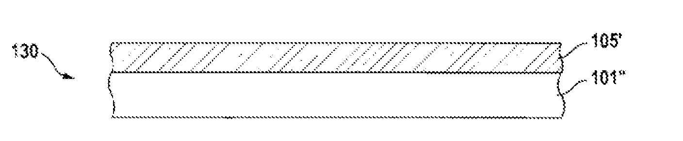
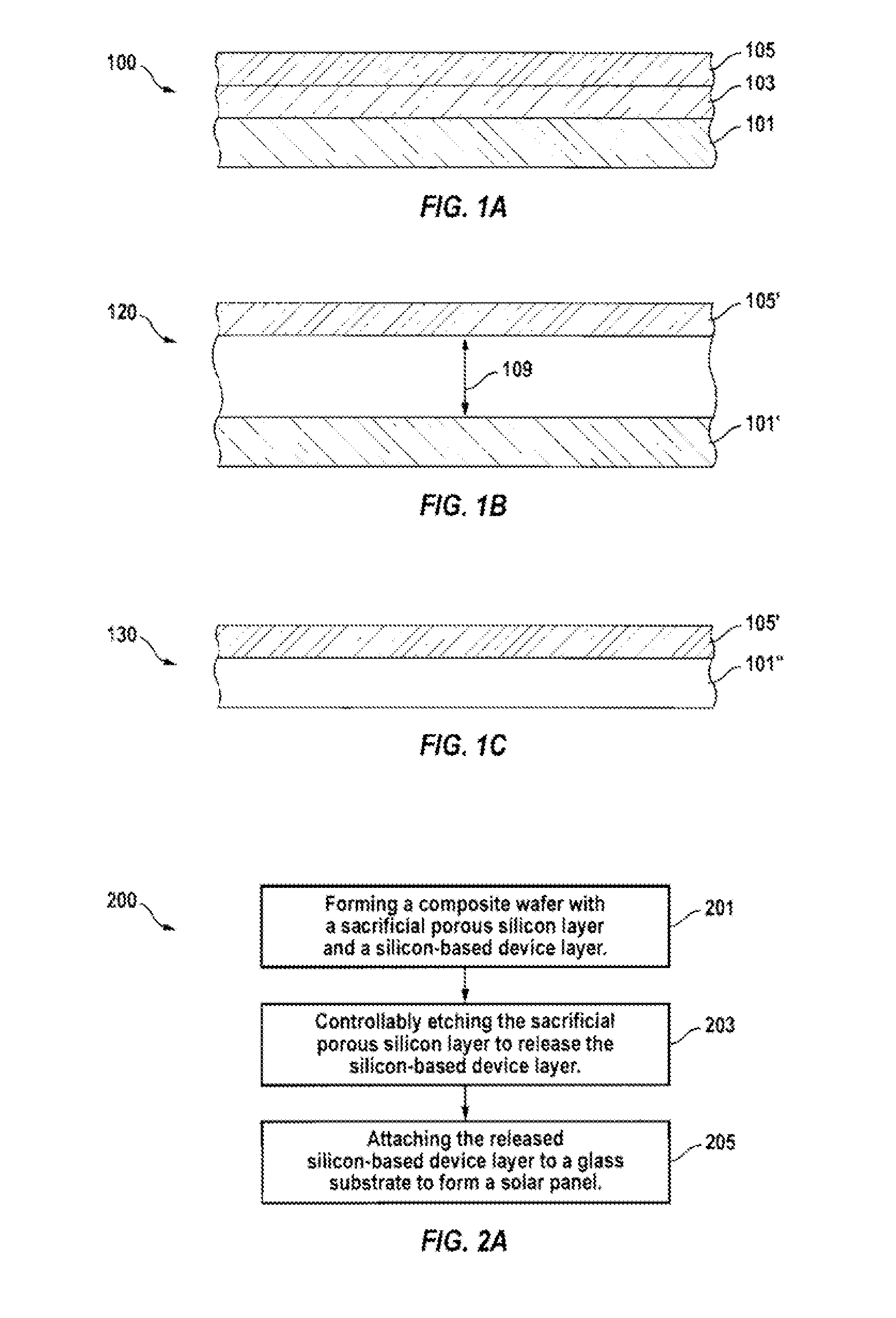
[0019]FIG. 1 shows a composite wafer 100 used to make a silicon-based device layer used in solar cells. The composite wafer 100 includes a single crystal silicon wafer 101 and a sacrificial porous silicon layer 103 that is deposited thereon, which is referred to herein as a base wafer. The composite wafer 100 also includes a silicon-based device layer 105 that is preferably crystalline or semi-crystalline and is epitaxially grown on top of the sacrificial porous silicon layer 103.

[0020]As described above, the sacrificial porous silicon layer 103 preferably has a porosity of 30 percent or more and is several nanometers to several microns thick. The sacrificial porous silicon layer 103 is formed from any suitable porous silicon material including, but not limited to carbon doped oxide, spin-on-glass (SOG), fluoridated silicon glass (FSG) or a combination thereof.

[0021]The silicon-based device layer 105 is preferably a p-doped silicon-based device layer that has a thickness of several ...


PUM

PropertyMeasurementUnit
temperatureaaaaaaaaaa
temperaturesaaaaaaaaaa

Abstract

A method for making a solar cell is disclosed. In accordance with the method of the present invention a composite wafer is formed. The composite layer includes a single crystal silicon wafer, a silicon-based device layer and sacrificial porous silicon sandwiched therebetween. The composite wafer is treated to an aqueous etchant maintained below ambient temperatures to selectively etch the sacrificial porous silicon and release or undercut the silicon-based layer from the single crystal silicon wafer. The released silicon device layer is attached to a substrate to make a solar cell and the released single crystal silicon wafer is reused to make additional silicon device layer.

Description

CROSS-REFERENCE TO RELATED APPLICATION[0001]The present application claims priority under 35 U.S.C. §119(e) to U.S. Provisional Patent Application Ser. No. 61 / 157,195, filed on Mar. 3, 2009, and titled “METHOD FOR SELECTIVE UNDER-ETCHING OF POROUS SILICON,” the entirety of which is hereby incorporated by reference.FIELD OF THE INVENTION[0002]This invention relates to a method for making solar cells. More particularly, the present invention relates to selective etching of a porous silicon layer to under-cut and release a silicon-based device layer that is then used for making solar cells.BACKGROUND OF THE INVENTION[0003]Solar cells are semiconductor devices that are usually manufactured from silicon-based material. Some solar cells are made from screen printed poly-crystalline silicon. Single crystalline wafers can be used to make very efficient solar cells. However, high manufacturing costs for making single crystalline materials makes the large scale production of solar cells from ...

Claims


Application Information

Patent Timeline
Patent Type & Authority Applications(United States)
IPC IPC(8): H01L21/20
CPCH01L21/31111H01L31/028Y02E10/547H01L31/1804H01L31/1892H01L31/068Y02P70/50H01L21/30604
Inventor KASHKOUSH, ISMAIL I.
Owner AKRION TECH
Why Eureka
Try Eureka