Precision separation of pv thin film stacks

a technology of pv thin film and stacking, which is applied in the field of system and method for manufacturing thin film panels, can solve the problems of manual positioning of cutting edge and width, overlay matching problems, etc., and achieve the effect of improving throughput, quality and cost of the final produ

Inactive Publication Date: 2010-09-16
IBM CORP
View PDF7 Cites 46 Cited by
  • Summary
  • Abstract
  • Description
  • Claims
  • Application Information

AI Technical Summary

Benefits of technology

[0004]The present invention solves the foregoing problems by providing a method for manufacturing thin film panels with a laser patterning system comprising: (a) providing a laser patterning system having a motorized translation stage, a computerized control system, an optical system including a single beam laser and a laser array, and a stepper motor operably coupled to the computerized control system and structured to cause movement of the translation stage; (b) depositing a base layer on top of a glass substrate; (c) separating the base layer by scribing a plurality of separation lines with the single beam laser, the plurality of separation lines corresponding with a predefined scribe pattern; (d) depositing a functional layer on top of the base layer; (e) determining a first base layer separation edge of the base layer using a refraction system that includes an infrared light source having a beam that is focused on a top surface of the functional layer; (f) operating the stepper motor to move the translation stage forward by a first distance; (g) activating the laser array and operating the stepper motor to move the translation stage forward by a second distance; (h) deactivating the laser array; (i) determining a subsequent base layer separation edge using the refraction system; (j) repeating steps (f)-(i) until the translation stage detects an end of the base layer; (k) when the translation stage detects the end of the base layer, depositing a top layer on top of the functional layer; (l) determining a first functional layer separation edge using the refraction system, wherein the beam of the infrared light source is focused on a top surface of the top layer; (m) operating the stepper motor to move the translation stage forward by a third distance upon detection of the first functional layer separation edge; (n) activating the laser array and operating the stepper motor to move the translation stage forward by a fourth distance; (o) deactivating the laser array; (p) determining a subsequent functional layer separation edge using the refraction system; and (q) repeating steps (m)-(p) until the translation stage detects an end of the functional layer. As will be appreciated by those skilled in the art, the present invention may improve throughput, quality and cost of the final product in a substantial manner.

Problems solved by technology

One disadvantage of this process results from the manual positioning of the cutting edge and the width.
Particularly, during the manufacturing process, surface patterning has to be applied several times (after each individual material deposition step) which can lead to overlay matching issues.

Method used


Image

  • Precision separation of pv thin film stacks
  • Precision separation of pv thin film stacks
  • Precision separation of pv thin film stacks

Examples


Embodiment Construction

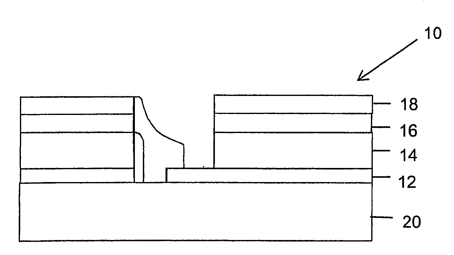
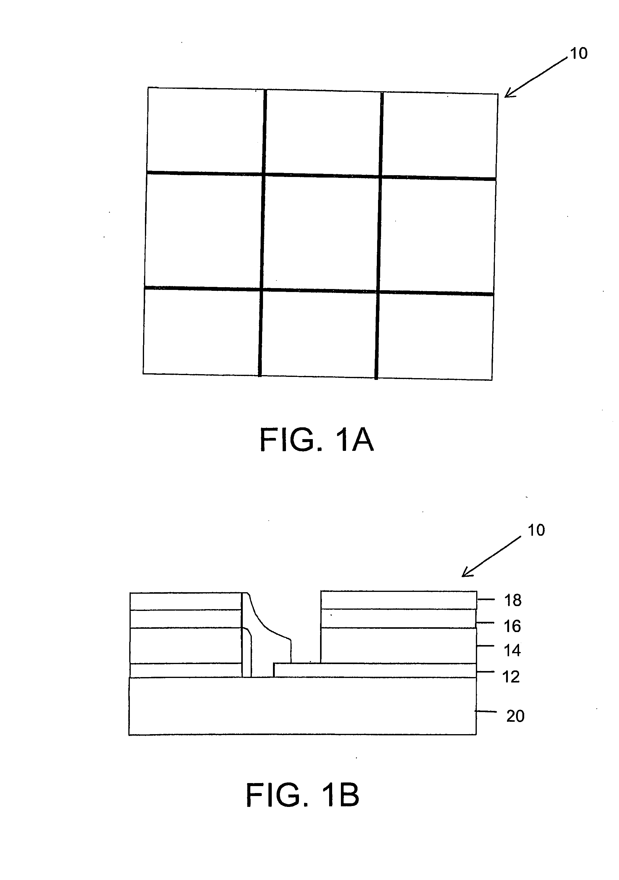
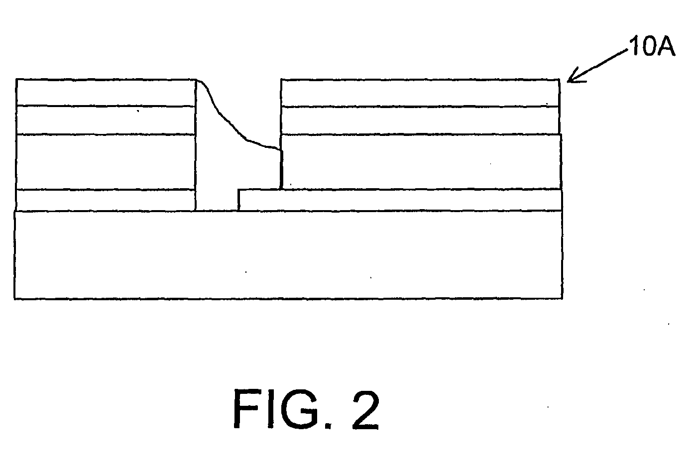
[0021]Generally speaking, the system and method of the present invention enable automated line cutting and formation of electrical contacts on deposited multi layer structures. The inventive concept may be applied to separate deposited multilayers into well defined segments as illustrated in FIGS. 1A-1B. In particular, FIG. 1A, is a diagram illustrating one exemplary multilayer panel 10 after the precision patterning steps of the present invention, while FIG. 1B is a side view illustrating a portion of the multilayer panel 10 of FIG. 1A. As illustrated in FIG. 1B, the multilayer panel 10 includes a base layer 12, a first functional layer 14, a second functional layer 16, and a top layer 18. The base layer 12 is positioned on top of a substrate 20. For purposes of comparison, FIG. 2 illustrates an exemplary multilayer panel 10A formed using a manual patterning process where the scribe lines are not perfectly aligned and result in quality issues including electrical shorts in the pane...


PUM

PropertyMeasurementUnit
thicknessaaaaaaaaaa
thicknessaaaaaaaaaa
thicknessaaaaaaaaaa

Abstract

A method for manufacturing thin film panels comprises providing a laser patterning system, depositing a base layer on a glass substrate, separating the base layer by scribing a plurality of separation lines corresponding with a predefined scribe pattern, depositing a functional layer on the base layer, determining a first base layer separation edge, moving the translation stage by a first distance, activating the laser array and moving the translation stage by a second distance, deactivating the laser array, determining subsequent separation edges of the base layer and scribing lines therein, depositing a top layer on the functional layer, determining a first functional layer separation edge, operating the stepper motor to move the translation stage by a third distance, activating the laser array and moving the translation stage by a fourth distance, deactivating the laser array, and determining subsequent separation edges of the functional layer and scribing lines therein.

Description

FIELD OF THE INVENTION[0001]The present invention generally relates to a system and method for manufacturing thin film panels. The present invention more specifically relates to a system and method using contrast recognition in order to achieve automated and precise alignment of a scribe pattern on a panel to overcome overlay matching problems.BACKGROUND OF THE INVENTION[0002]Several industrial applications require the separation of large area structures into smaller sub-structures. One common example is the structuring of thin film solar panels formed on glass substrates. With regard to the formation of thin film solar panels, surface patterning is used to define individual areas or cells, while at the same time monolithically integrating the individual cells of a panel to provide a specific output voltage. A key requirement of surface patterning is to minimize the scribe area in order to maximize the active area and efficiency of a module. Typically, the efficiency of a module is ...

Claims


Application Information

Patent Timeline
Patent Type & Authority Applications(United States)
IPC IPC(8): B05D5/12
CPCB23K26/045H01L31/022425H01L31/046Y02E10/50H01L31/0392B23K26/044H01L31/03923H01L31/0465Y02E10/541Y02P70/50
Inventor KRAUSE, RAINERPFEIFFER, GERD
Owner IBM CORP
Why Eureka
Try Eureka