Chip Guard Ring Including a Through-Substrate Via

a chip guard and through-substrat via technology, applied in the direction of semiconductor devices, semiconductor/solid-state device details, electrical apparatus, etc., can solve the problems of difficult design of compact high-performance semiconductor chips, degraded circuit performance, etc., to achieve the effect of minimizing the area sufficient grounding of the semiconductor chip, and improving the performance of the semiconductor chip

Active Publication Date: 2010-09-23
TESSERA INC
View PDF20 Cites 61 Cited by
  • Summary
  • Abstract
  • Description
  • Claims
  • Application Information

AI Technical Summary

Benefits of technology

[0004]The present invention provides a semiconductor structure that enables sufficient grounding of a semiconductor chip's seal ring without employing grounding metal pads, and thereby minimizing the area for the semiconductor

Problems solved by technology

Excessive reduction in the number of the grounding metal pads may result in degraded circuit performance through insufficient blocking of spurious signals to the gu

Method used


Image

  • Chip Guard Ring Including a Through-Substrate Via
  • Chip Guard Ring Including a Through-Substrate Via
  • Chip Guard Ring Including a Through-Substrate Via

Examples


first embodiment

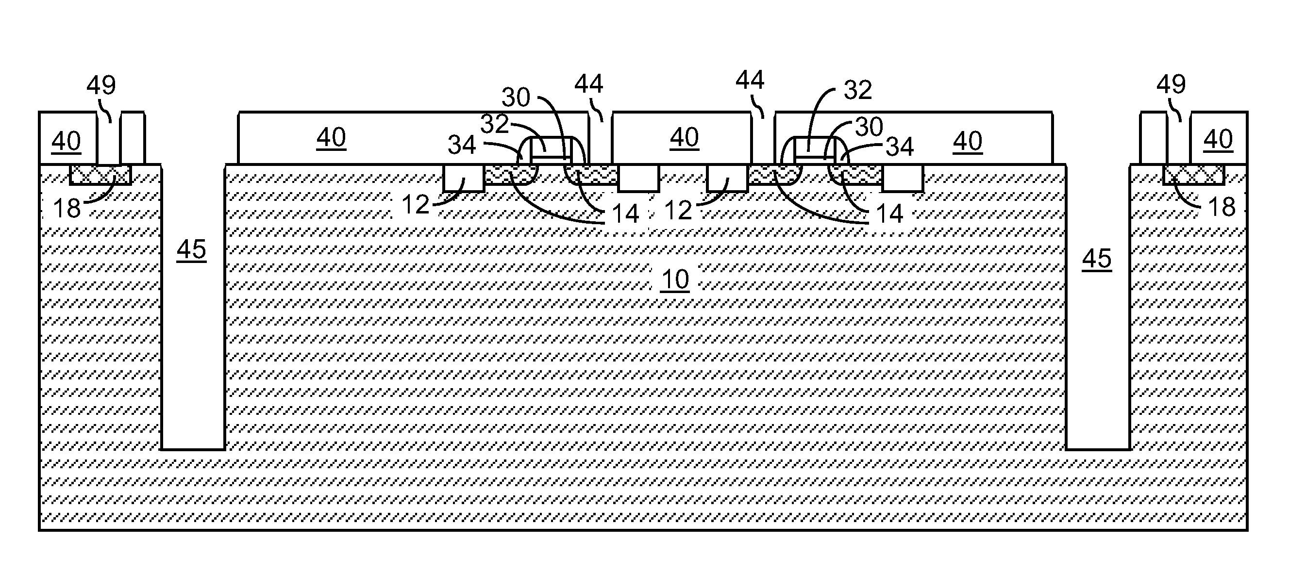
[0013]Referring to FIG. 1, a first exemplary structure according to the present invention includes a semiconductor substrate 10 having at least one semiconductor device formed on a surface thereof. For example, the at least one semiconductor device may include a field effect transistor including source and drain regions 14, a gate dielectric 30, a gate electrode 32, and a gate spacer 34. Shallow trench isolation structures 12 may provide electrical separation between semiconductor devices.

[0014]The semiconductor substrate 10 includes a semiconductor material, which may be selected from, but is not limited to, silicon, germanium, silicon-germanium alloy, silicon carbon alloy, silicon-germanium-carbon alloy, gallium arsenide, indium arsenide, indium phosphide, III-V compound semiconductor materials, II-VI compound semiconductor materials, organic semiconductor materials, and other compound semiconductor materials. For example, the semiconductor material may comprise single crystalline...

third embodiment

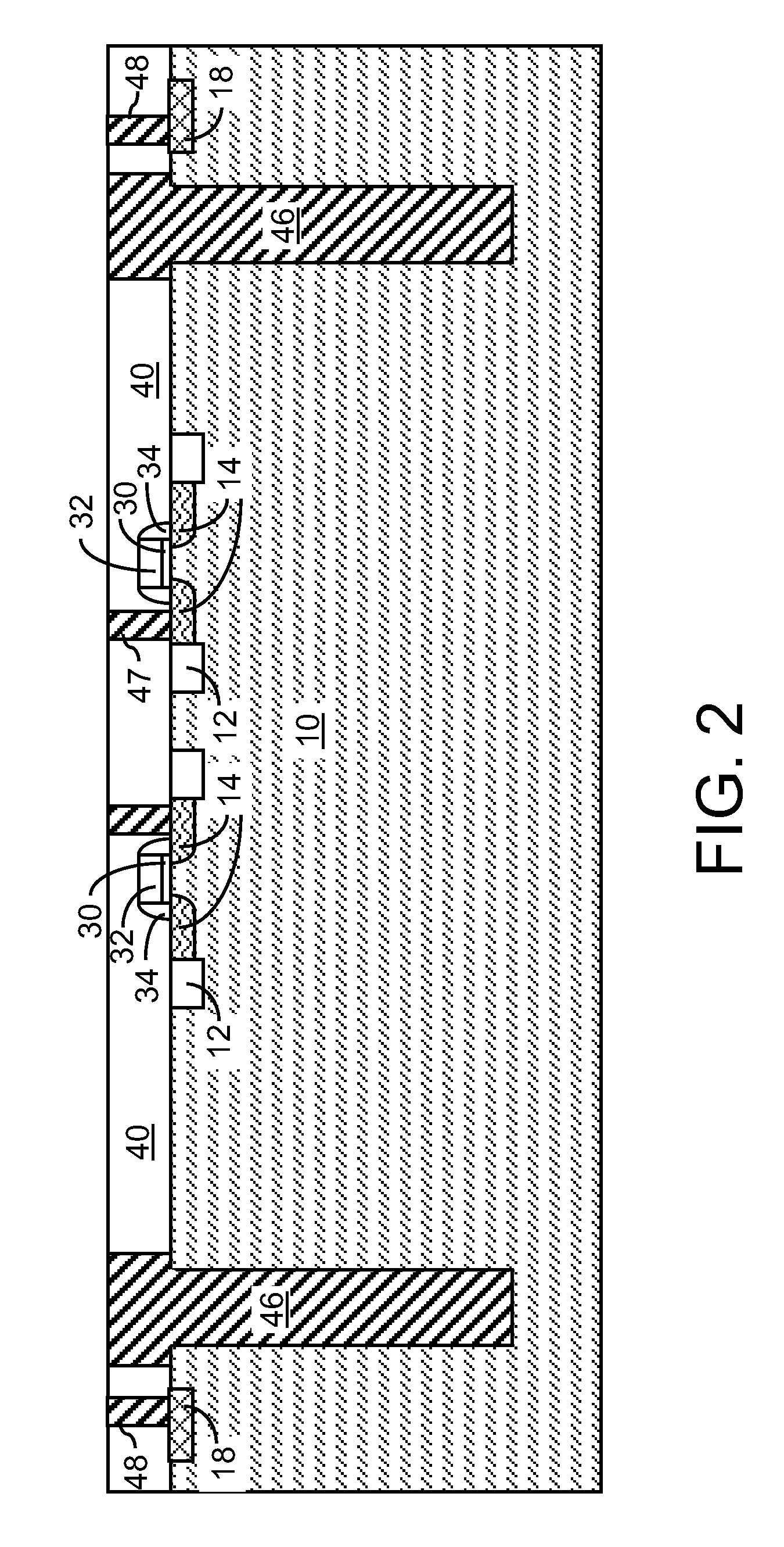
[0041]In the third embodiment, the at least one through-substrate via 46 is a plurality of through-substrate vias. Each through-substrate via in the plurality of through-substrate vias does not abut one another. All other elements of the third exemplary semiconductor structure may be the same as in the first exemplary semiconductor structure.

[0042]The plurality of through substrate vias is formed in peripheral area of the third exemplary semiconductor structure. The third exemplary semiconductor structure may be a semiconductor die (semiconductor chip) or a semiconductor chiplet included in a semiconductor die. Correspondingly, the peripheral area of the third exemplary semiconductor structure may be a peripheral area of a semiconductor chip or a peripheral area of a semiconductor chiplet contained within a semiconductor chip. The at least one through-substrate via 46 in the form of a plurality of through substrate vias in the third exemplary semiconductor structure enhances electri...


PUM


Abstract

At least one through-substrate via is formed around the periphery of a semiconductor chip or a semiconductor chiplet included in a semiconductor chip. The at least one through-substrate via may be a single through-substrate via that laterally surrounds the semiconductor chip or the semiconductor chiplet, or may comprise a plurality of through-substrate vias that surrounds the periphery with at least one gap among the through-substrate vias. A stack of back-end-of-line (BEOL) metal structures that laterally surrounds the semiconductor chip or the semiconductor chiplet are formed directly on the substrate contact vias and electrically connected to the at least one through-substrate via. A metallic layer is formed on the backside of the semiconductor substrate including the at least one through-substrate via. The conductive structure including the metallic layer, the at least one through-substrate via, and the stack of the BEOL metal structures function as an electrical ground built into the semiconductor chip.

Description

FIELD OF THE INVENTION[0001]The present invention relates to semiconductor structures, and particularly to a chip guard ring (also called a chip seal ring or a die seal) structure including a through-substrate via, and methods of manufacturing the same.BACKGROUND OF THE INVENTION[0002]A chip guard ring typically comprises a stack of back-end-of-line (BEOL) metal interconnect structures that are located on an outer periphery of a semiconductor chip. The chip guard ring functions as a metal seal against ionic contaminants. The chip guard ring also functions as a low resistance path between electrical ground nodes of semiconductor devices on the semiconductor substrate and grounding metal pads located on the top surface of dielectric layers including back-end-of-line metal interconnect structures of the semiconductor chip. Typically, multiple grounding metal pads are required to provide adequate grounding of the semiconductor chip's guard ring. The grounding metal pads may be C4 flip c...

Claims


Application Information

Patent Timeline
IPC IPC(8): H01L23/48H01L21/768
CPCH01L21/743H01L21/76898H01L23/481H01L23/5225H01L23/585H01L29/78H01L2924/0002H01L2924/12044H01L2924/00012H01L2924/00
Inventor GILLIS, JOHN D.NI, WAN
Owner TESSERA INC
Why Eureka
Try Eureka