Doping and milling of granular silicon

a technology of granular silicon and milling chamber, which is applied in the direction of non-metal conductors, conductors, silicon compounds, etc., can solve the problems of high cost of conventional monocrystalline silicon wafers. , to achieve the effect of widespread use as an economical replacement for commercial power, solar cells can be effectively and widely deployed as economical replacements for commercial power, and the silicon parts

Inactive Publication Date: 2010-09-30
INTEGRATED PHOTOVOLTAICS
View PDF5 Cites 36 Cited by
  • Summary
  • Abstract
  • Description
  • Claims
  • Application Information

AI Technical Summary

Benefits of technology

[0012]The roller milling system and its feed system are advantageously disposed within an environmental chamber back filled with an inert gas such ...

Problems solved by technology

Solar cells can also be made in such wafers, but the conventional monocrystalline silicon wafers are generally considered to be too expensive for solar cells to be effectively and widely deployed as an economical replacement for commercial power.
However, further development work in ou...

Method used


Image

  • Doping and milling of granular silicon
  • Doping and milling of granular silicon
  • Doping and milling of granular silicon

Examples


Embodiment Construction

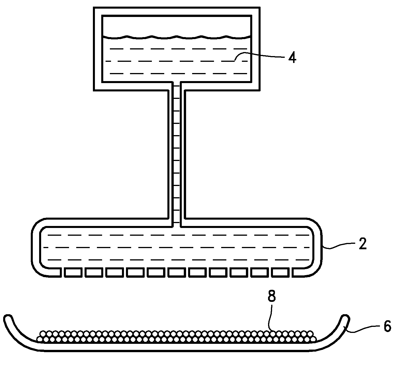
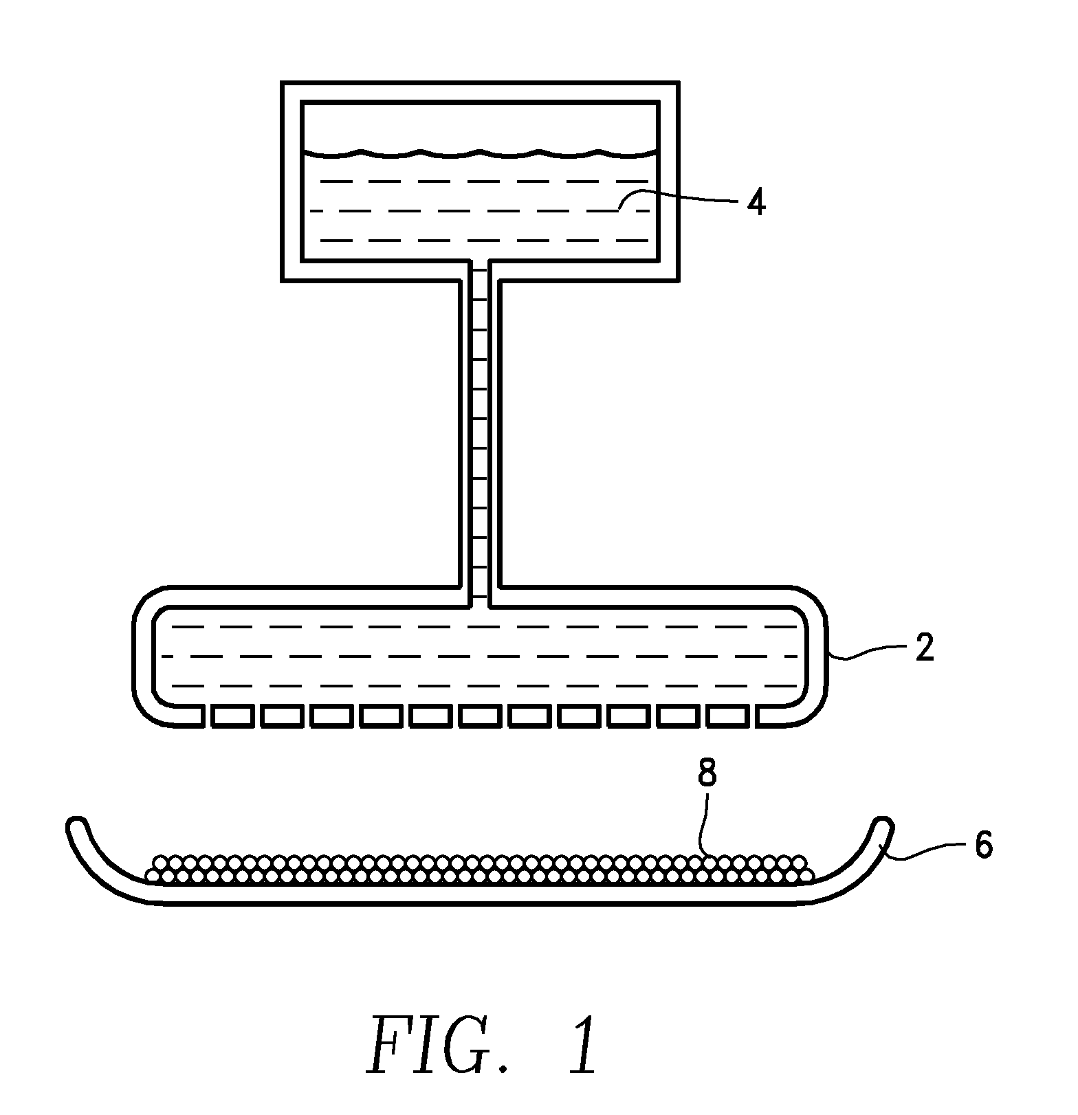
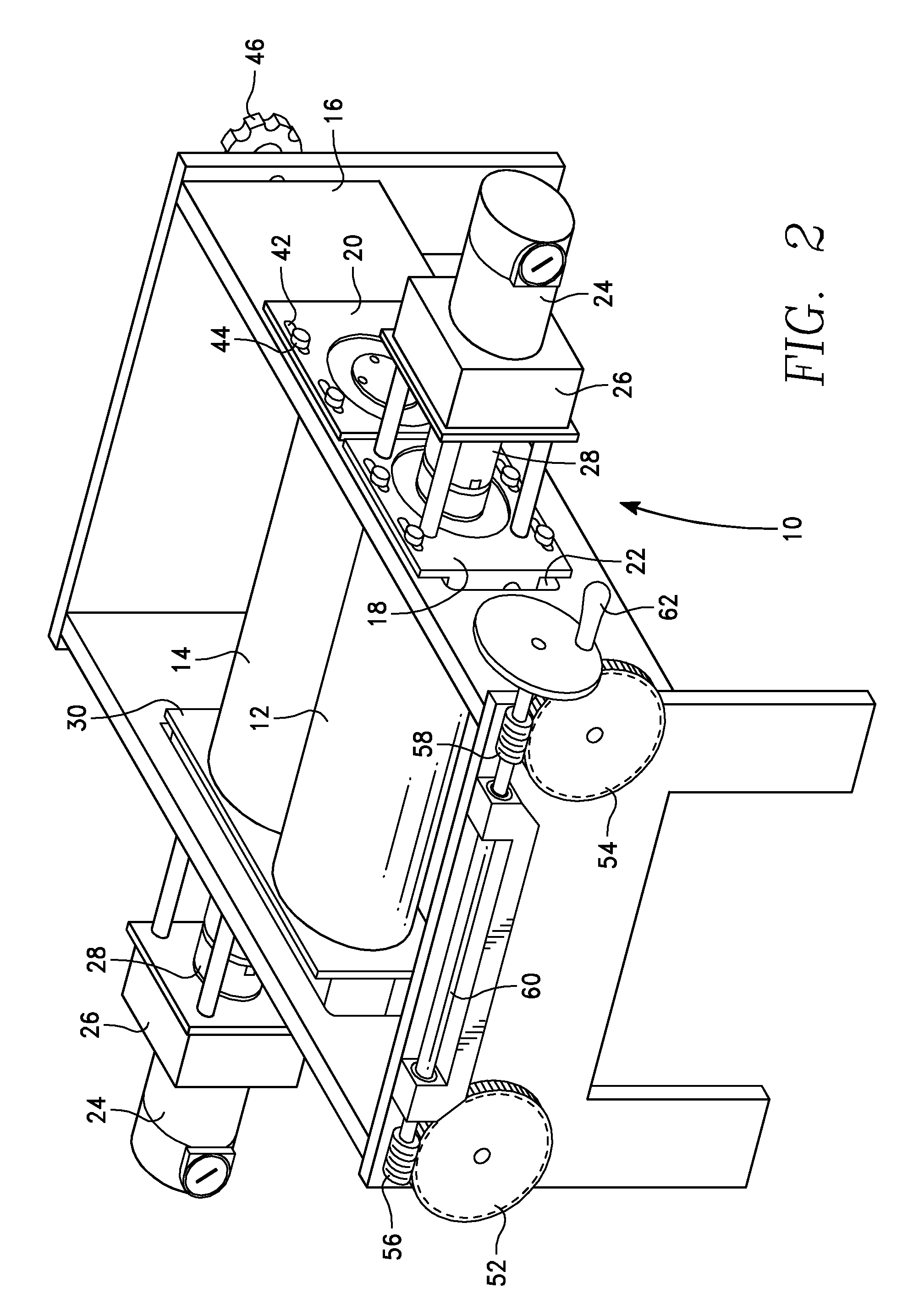
[0019]Different aspects of the invention include mechanical grinding or crushing of silicon pieces to small particles of high purity and of controlled size and the semiconductor doping of such silicon particles. The mechanical grinding may be followed by an optional sieving and subsequent jet milling of the particles into yet smaller silicon powder. However, the silicon feedstock must be highly pure and the purity should be maintained during the grinding process.

[0020]The semiconductor industry has promoted the development of economical production of electronic grade silicon (EGS) of very high purity. In the usual Siemens process, gaseous precursors of hydrogen and trichlorosilane are injected into a reactor containing a hot seed rod of silicon. The precursors in a chemical vapor deposition (CVD) process deposit onto the seed rod as growing layers of polysilicon silicon to form a rod or ingot of EGS, also called virgin polysilicon. The growth conditions favor the formation of high s...


PUM


Abstract

Doped silicon particles, including powder suitable for plasma spraying semiconductor devices, is formed by liquid doping applied to larger particles, which are then milled to a smaller size. Doped or undoped silicon may be milled by a roller mill including silicon rollers and advantageously having feed and collection systems formed of silicon and operated in a nitrogen ambient. A two-stage system includes sieving the rolled product for further size reduction in a jet mill.

Description

RELATED APPLICATION[0001]This application claims benefit of provisional application 61 / 165,218, filed Mar. 31, 2009.FIELD OF THE INVENTION[0002]The invention relates generally to producing silicon grains forming a powder useful for plasma spraying semiconducting devices such as solar cells. In particular, the invention relates to both the doping and milling of such silicon powder.BACKGROUND ART[0003]Integrated circuits based upon semiconducting silicon have conventionally been formed in monocrystalline silicon wafers cut from ingots grown by the Czochralski method, which includes pulling the ingot from a melt of pure silicon. Solar cells can also be made in such wafers, but the conventional monocrystalline silicon wafers are generally considered to be too expensive for solar cells to be effectively and widely deployed as an economical replacement for commercial power. As a result, much recent effort has been directed to developing economical techniques for depositing a semiconductor...

Claims


Application Information

Patent Timeline
IPC IPC(8): H01B1/04C01B33/02B05D1/02B02C13/02B02C23/02
CPCB02C4/02B02C4/283C01B33/02B02C4/30B02C4/286
Inventor ZEHAVI, RAANAN
Owner INTEGRATED PHOTOVOLTAICS
Why Eureka
Try Eureka