Substrate processing apparatus, substrate processing method, and computer-readable storage medium

Active Publication Date: 2010-10-14
TOKYO ELECTRON LTD
View PDF9 Cites 50 Cited by
  • Summary
  • Abstract
  • Description
  • Claims
  • Application Information

AI Technical Summary

Benefits of technology

[0031]In one aspect of the invention, the present disclosure provides a substrate processing apparatus and a substrate processing method which are adapted to rotate a substrate around the axis of a turntable relative to the gas supplying uni

Problems solved by technology

Hence, although the ALD can inherently provide excellent uniformity of the film thickness in the surface, the above-described film deposition device may not be able to demonstrate the advantageous feature thereof sufficiently.
In order to fill the cavity internally formed in the recess, a high heating temperature and a long processing time are needed.
This process may result in a lowering of the throughput, and there may be a probability that a severe thermal history be given to the device structure which is already formed.
When the ALD method is performed, good embedding characteristics are provided inherently, but because

Method used


Image

  • Substrate processing apparatus, substrate processing method, and computer-readable storage medium
  • Substrate processing apparatus, substrate processing method, and computer-readable storage medium
  • Substrate processing apparatus, substrate processing method, and computer-readable storage medium

Examples


first embodiment

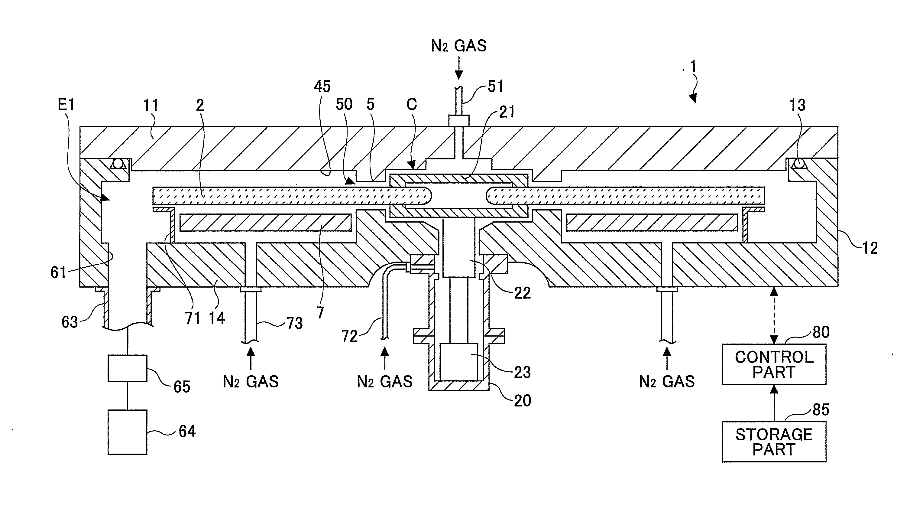
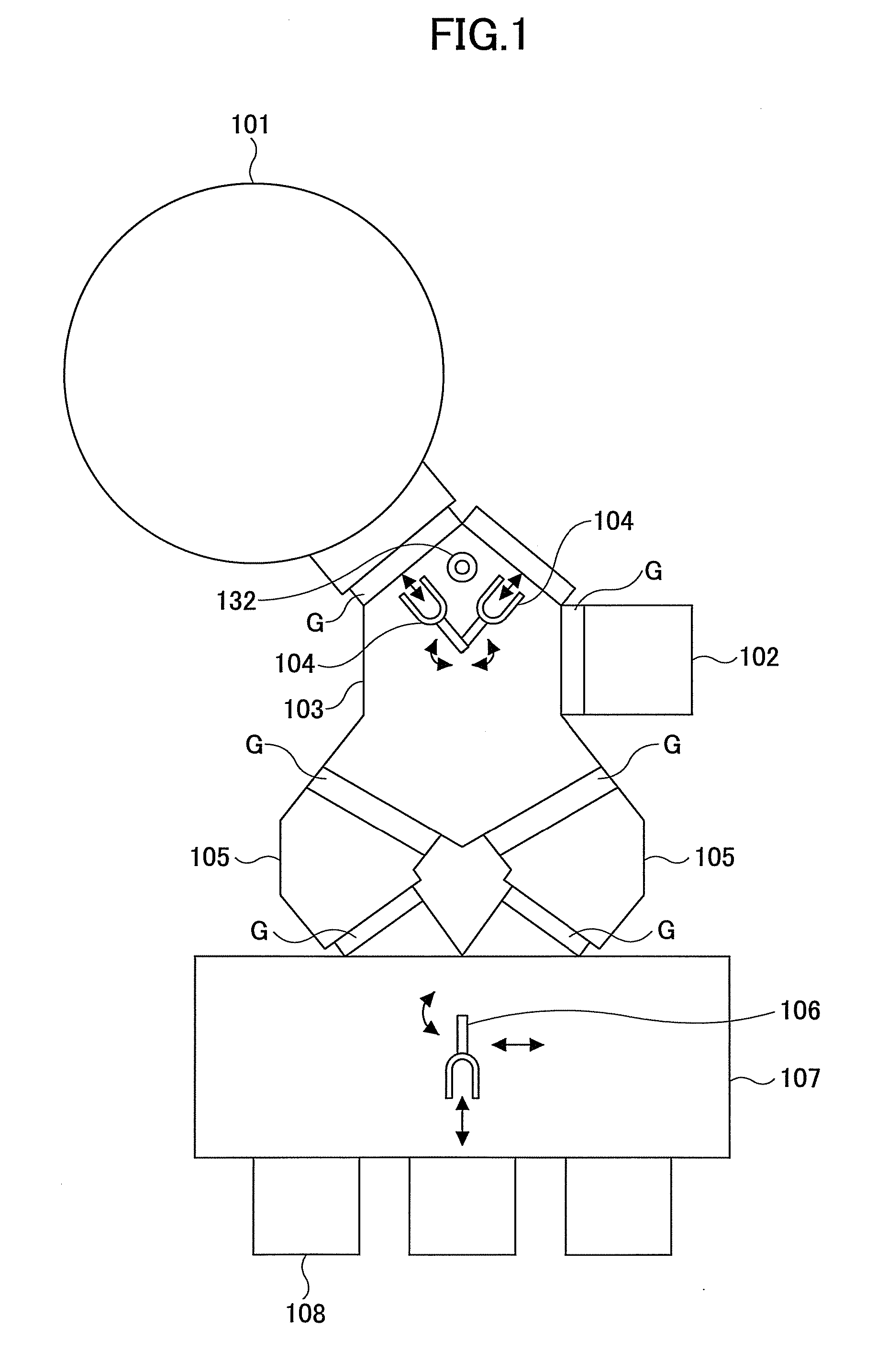
[0069]FIG. 1 illustrates the composition of a substrate processing apparatus of the invention. The substrate processing apparatus of this embodiment includes a film deposition device 101 for performing a film deposition process of a substrate W (which is, for example, a semiconductor wafer, also called a wafer W) to form thereon a thin film which is made of at least a silicon oxide, a heat processing device 102 for performing an anneal processing (or heat processing) to the wafer W, and a vacuum conveying chamber 103 which is airtightly connected between the film deposition device 101 and the heat processing device 102.

[0070]A conveyance opening 15 for delivering the wafer W is formed in the surface of a wall between the film deposition device 101 and the heat processing device 102, which will be described later. Through an exhaust passage in which a pressure regulation part which is constituted by, for example, a butterfly valve is arranged, the inside of the vacuum conveying chamb...

second embodiment

[0158]Next, the invention will be described with reference to FIG. 20.

[0159]In this embodiment, at least one of boron (B) and phosphorus (P) is contained in the silicon oxide film 242 and mixed therewith so that the silicon oxide film 242 is made to reflow promptly.

[0160]The composition of a film deposition device of this embodiment will be described. In this film deposition device, the compound which contains one of boron and phosphorus (for example, the compound containing phosphorus, or PH3(phosphine) gas) is supplied to the wafer as the third reactive gas. The third gas nozzle 280 which is made of, for example, quartz is arranged as a third reactive gas supplying unit, and the nozzle 280 is disposed between the second reactive gas nozzle 32 and the conveyance opening 15 in the direction of rotation of the turntable 2.

[0161]The nozzle 280 is constructed similar to each of the nozzles 31, 32, 200, 41 and 42 described above. The nozzle 280 is attached to face the wafer W so that th...

third embodiment

[0174]Next, the invention will be described. This embodiment is suitably applicable when forming a high derivative (high-k) film, such as a STO film. In this embodiment, the reactive gases supplied from the nozzles 31 and 32 are, for example, a Ti(MPD)(THD) 2 gas and a Sr(THD)2 gas, respectively. In this case, the heating temperature of the wafer W in the heat processing device 102 is set to a temperature in a range of 300 degrees C.-400 degrees C.


PUM


Abstract

In a substrate processing apparatus, a film deposition device and a heat processing device to perform an anneal processing are airtightly connected to a vacuum conveying chamber, and a substrate rotating unit to cause a substrate to rotate around a vertical axis is provided in the vacuum conveying chamber. A control unit is arranged to stop a relative rotation of a plurality of reactive gas supplying units, a separating gas supplying unit and a table by a rotation device in the middle of a film deposition process of the substrate, cause a conveying unit to take out the substrate from a vacuum chamber, and output a control signal that causes a substrate rotating unit to change a direction of the substrate.

Description

CROSS-REFERENCE TO RELATED APPLICATION[0001]This application is based upon and claims the benefit of priority of Japanese patent application No. 2009-095213, filed on Apr. 9, 2009, the entire contents of which are incorporated by reference in their entirety.BACKGROUND OF THE INVENTION[0002]1. Field of the Invention[0003]This invention relates to a substrate processing apparatus, a substrate processing method, and a computer-readable storage medium which are adapted to laminate layers of resultants of mutually reactive gases to form a thin film on a substrate by performing a gas supply cycle which supplies the reactive gases sequentially to a surface of the substrate in a vacuum chamber.[0004]2. Description of the Related Art[0005]As a film deposition technique in a semiconductor fabrication process, a technique of forming a thin film is known which sequentially supplies at least two kinds of mutually reactive gas in a vacuum pressure atmosphere to a semiconductor wafer (also called ...

Claims


Application Information

Patent Timeline
IPC IPC(8): C23C16/52C23C16/00C23C16/44
CPCH01L21/67109H01L21/6719H01L21/67207C23C16/52H01L21/68771C23C16/54H01L21/68764
Inventor KATO, HITOSHIHONMA, MANABUKIKUCHI, HIROYUKI
Owner TOKYO ELECTRON LTD
Why Eureka
Try Eureka