Nonvolatile memory electronic device including nanowire channel and nanoparticle-floating gate nodes and a method for fabricating the same

a technology of nonvolatile memory and electronic devices, which is applied in the field of nonvolatile memory electronic devices including nanowire channels and nanoparticle-floating gate nodes, can solve the problems of reducing the size of cells, difficult to satisfy the demand required by the world, and various existing flash memory devices, so as to improve the degree of integration, improve the property of channels, and reduce the channel used in transporting charge carriers

Inactive Publication Date: 2010-11-04
INTELLECTUAL DISCOVERY CO LTD
View PDF11 Cites 51 Cited by
  • Summary
  • Abstract
  • Description
  • Claims
  • Application Information

AI Technical Summary

Benefits of technology

[0018]The present device and method are conceived to solve the aforementioned problems of existing memory devices. An object is to provide a memory electronic device including nanowire channel and nanoparticle-floating gate nodes and a method for manufacturing the same, inter alia. The memory electronic device including nanowire channel and nanoparticle-floating gate nodes is configured by forming nanoparticles on a surface of a tunneling layer formed to cover a nanowire such that the nanoparticles cover the nanowire and the tunneling layer. At this time, a degree of integration is improved by reducing channels used in transporting charge carriers using a nanowire, and a property of the channels is improved using a nanowire with excellent charge mobility. In addition, nanoparticles used as a charge trapping layer enable the device to be operated even at a low voltage, and thus, the thickness of the tunneling and insulating layers is reduced, thereby improving a degree of integration of the device.
[0019]Another object is to provide a memory electronic device including nanowire channel and nanoparticles-floating gate nodes and a method for manufacturing the same, wherein a gate structure used in a nonvolatile memory device is changed from an existing one-dimensional planar structure shape to a gate structure shape, such as top, omega and cylinder shapes, so that on / off property, subthreshold swing effect and mobility of charge carriers in the device are maximized according to the change of the gate structure, thereby providing a faster device operating speed and a low operating voltage. In addition, the method is simpler and less expensive than an existing top-down type fabrication process.

Problems solved by technology

It is considered that such a technology will become a growth factor of economic and industrial development in the future, and it will be difficult to satisfy the demand required by the world if a development rate of such a technology is slowed down.
Existing flash memory devices have various problems when the size of cells are decreased, since the existing flash memory devices require a high operating voltage.
Therefore, there is a limit to the extent that the size of existing flash memory can be decreased.
However, since many defects of the SiO2 thin film forming leakage paths make charge carriers difficult to be trapped in the floating gate nodes.
If several program / erase processes are performed at such a high voltage, a thin tunneling layer will be broken, creating a leakage path for charge carriers in the floating gate layer and causing the tunneling layer to lose its function.
However, when the tunneling layer is partially broken, a large leakage current is generated while charge carriers in the charge trapping layer flow into the channels through the damaged tunneling layer.
The existing devices further have the disadvantage of exhibiting poor endurance since the tunneling layer is considerably damaged as the program / erase processes are performed many times.
However, there is a problem that the thicker tunneling and insulating layers deteriorate the degree of integration of a device and require a high program / erase voltage.

Method used


Image

  • Nonvolatile memory electronic device including nanowire channel and nanoparticle-floating gate nodes and a method for fabricating the same
  • Nonvolatile memory electronic device including nanowire channel and nanoparticle-floating gate nodes and a method for fabricating the same
  • Nonvolatile memory electronic device including nanowire channel and nanoparticle-floating gate nodes and a method for fabricating the same

Examples


first embodiment

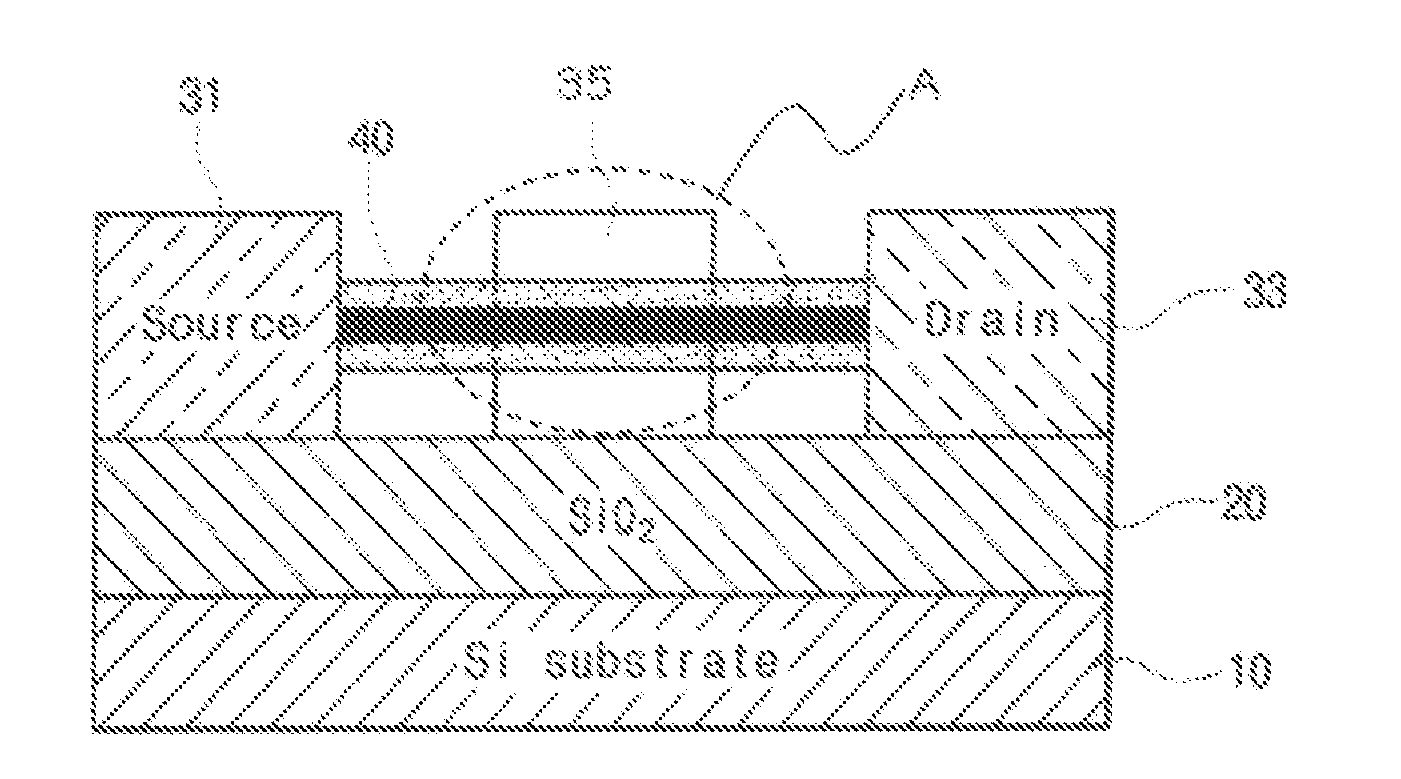
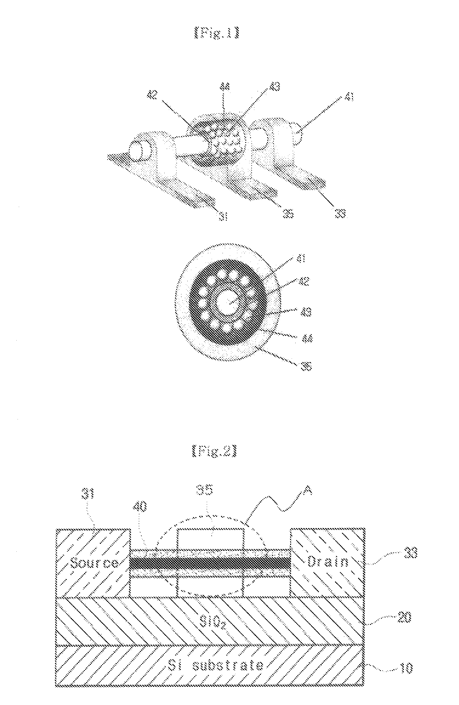
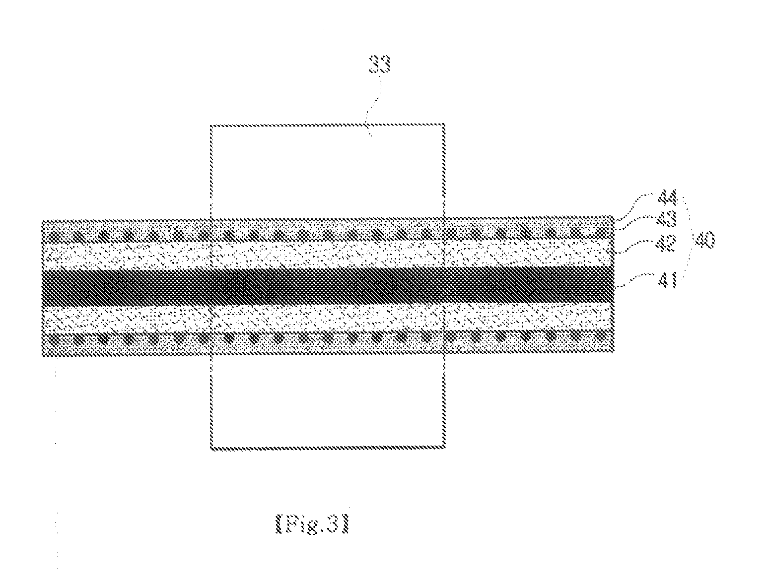
[0065]A fabrication method of a nonvolatile memory electronic device including nanowire channel and nanoparticles-floating gate nodes according to a first embodiment of the present invention comprises steps of preparing a semiconductor nanowire composite, forming a gate electrode in a central part of a semiconductor nanowire composite by a photolithography or electron beam lithography method, applying a sample of the nanowire composite / gate electrode formed nanowire composite to a SiO2 capped silicon, semiconductor, glass or plastic substrate, and forming source and drain electrodes on both ends of the nanowire on the substrate by a photolithography or electron beam lithography method.

[0066]Here, the step of preparing a semiconductor nanowire composite includes steps of coating a semiconductor nanowire with a tunneling layer of an insulating material by an atomic layer deposition method, of an organic insulating material, and of an insulating layer by a sputtering method or a chemic...

second embodiment

[0077]Referring to FIGS. 7a to 7g, a fabrication process of a nonvolatile memory electronic device including nanowire channel and nanoparticles-floating gate nodes according to a second embodiment of the present invention will be described. First, referring to FIG. 7a, semiconductor nanowires 41 are dispersed on the hexamethyldisilazane (HMDS) film 21, deposited on a silicon, semiconductor, glass, or plastic substrate 10 not only to increase adhesive force between the photoresist layer and substrate but also to serve as a sacrificial layer for the semiconductor nanowire 41 to be floated from the substrate, then the first photoresist layer 51 is spin-coated onto the semiconductor nanowire-dispersed HMDS film. Resist patterns in the range from several μm to several tens of nm for the formation of electrodes are made after exposure and development processes. That is, a first space portion (not shown,) in which source and drain electrodes to be described later are formed, is formed usin...

third embodiment

[0093]Hereinafter, a fabrication process of a nonvolatile memory electronic device including nanowire channel and nanoparticles-floating gate nodes according to a third embodiment of the present invention will be described referring to FIGS. 10a to 10g of the accompanying drawings.

[0094]There are two methods for manufacturing a nanowire. The first one is, according to any one of existing methods, to grow semiconductor nanowires on a substrate, which is preferably made of a Si or Al2O3 material. According to another method for manufacturing the nanowire, a semiconductor substrate is patterned by a photolithography method or an electron beam lithography method, and then the patterned semiconductor substrate is etched to have a predetermined thickness and width through an etching method, thereby manufacturing a nanowire.

[0095]As described above, after growing a semiconductor nanowire on the substrate, a tunneling layer 42 is deposited on a surface of the grown semiconductor nanowire us...


PUM

PropertyMeasurementUnit
thicknessaaaaaaaaaa
temperatureaaaaaaaaaa
thicknessaaaaaaaaaa

Abstract

A nonvolatile memory electronic device including nanowire channel and nanoparticle-floating gate nodes, in which the nonvolatile memory electronic device, which comprises a semiconductor nanowire used as a charge transport channel and nanoparticles used as a charge trapping layer, is configured by allowing the nanoparticles to be adsorbed on a tunneling layer deposited on a surface of the semiconductor nanowire, whereby charge carriers moving through the nanowire are tunneled to the nanoparticles by a voltage applied to a gate, and then, the charge carriers are tunneled from the nanoparticles to the nanowire by the change of the voltage that has been applied to the gate, whereby the nonvolatile memory electronic device can be operated at a low voltage and increase the operation speed thereof.

Description

CROSS-REFERENCE TO RELATED APPLICATIONS[0001]The benefit of priority is claimed to Republic of Korea Patent Applications No. 10-2007-0018271 and 10-2007-0018259, both of which were filed with the Korean Intellectual Property Office on Feb. 23, 2007, and both of which are incorporated by reference herein in their entireties.BACKGROUND[0002]1. Technical Field[0003]The present discussion relates to a nonvolatile memory electronic device and a method for manufacturing the same, and more particularly, to a nonvolatile memory electronic device including nanowire channel and nanoparticles-floating gate nodes and a method for manufacturing the same, in which the nonvolatile memory electronic device, which includes a semiconductor nanowire used as a charge transport channel and nanoparticles used as a charge trapping layer, is configured by allowing the nanoparticles to be adsorbed on a tunneling layer deposited on a surface of the semiconductor nanowire, such that charge carriers moving thr...

Claims


Application Information

Patent Timeline
Patent Type & Authority Applications(United States)
IPC IPC(8): H01L29/792H01L21/336
CPCB82Y10/00H01L29/792G11C13/0014G11C13/025G11C2213/17G11C2213/18H01L29/0665H01L29/0673H01L29/068H01L29/42332H01L29/42348H01L29/42392H01L29/775H01L29/78681H01L29/78684H01L29/7869H01L29/7881G11C11/5664G11C11/5671
Inventor KIM, SANGSIGYOON, CHANG JUNJEONG, DONG YOUNGYEOM, DONG HYUK
Owner INTELLECTUAL DISCOVERY CO LTD
Why Eureka
Try Eureka